Display device and method for manufacturing the same

a technology of display device and flat panel, which is applied in the direction of semiconductor device, electrical apparatus, instruments, etc., can solve the problems of deterioration of contrast and visibility, increase of flat panel display device thickness, additional process, etc., and achieve the effect of improving contrast and visibility and enhancing process efficiency

Active Publication Date: 2016-04-26
SAMSUNG DISPLAY CO LTD
View PDF22 Cites 2 Cited by
  • Summary
  • Abstract
  • Description
  • Claims
  • Application Information

AI Technical Summary

Benefits of technology

[0011]Aspects of some embodiments of the present invention are directed toward a display device improved in contrast and visibility and capable of enhancing process efficiency, and to a method of manufacturing the display device.
[0034]According to some embodiments of the present invention, a display device may include a metal pattern formed on a thin film encapsulation layer overlapping a pixel defining layer, thereby preventing or reducing external-light reflection and improving outdoor visibility.
[0035]Further, according to some embodiments of the present invention, a method of manufacturing the display device may minimize or reduce a general photolithography process, thereby improving process efficiency and preventing or reducing damages on the thin film encapsulation layer.

Problems solved by technology

If the user views the flat panel display devices outdoors, sunlight is reflected off the flat panel display devices, which causes deterioration in contrast and visibility.
However, the circular polarizer may lead to an increase in the thickness of the flat panel display device, and may also require an additional process.

Method used


Image

  • Display device and method for manufacturing the same
  • Display device and method for manufacturing the same
  • Display device and method for manufacturing the same

Examples


Embodiment Construction

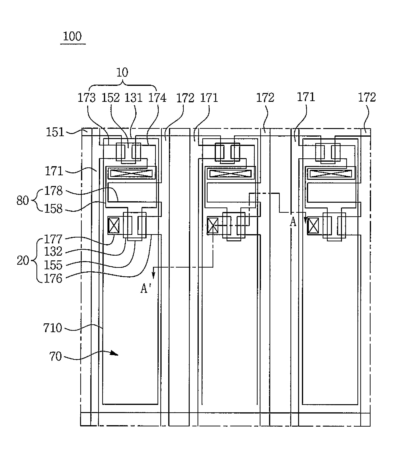
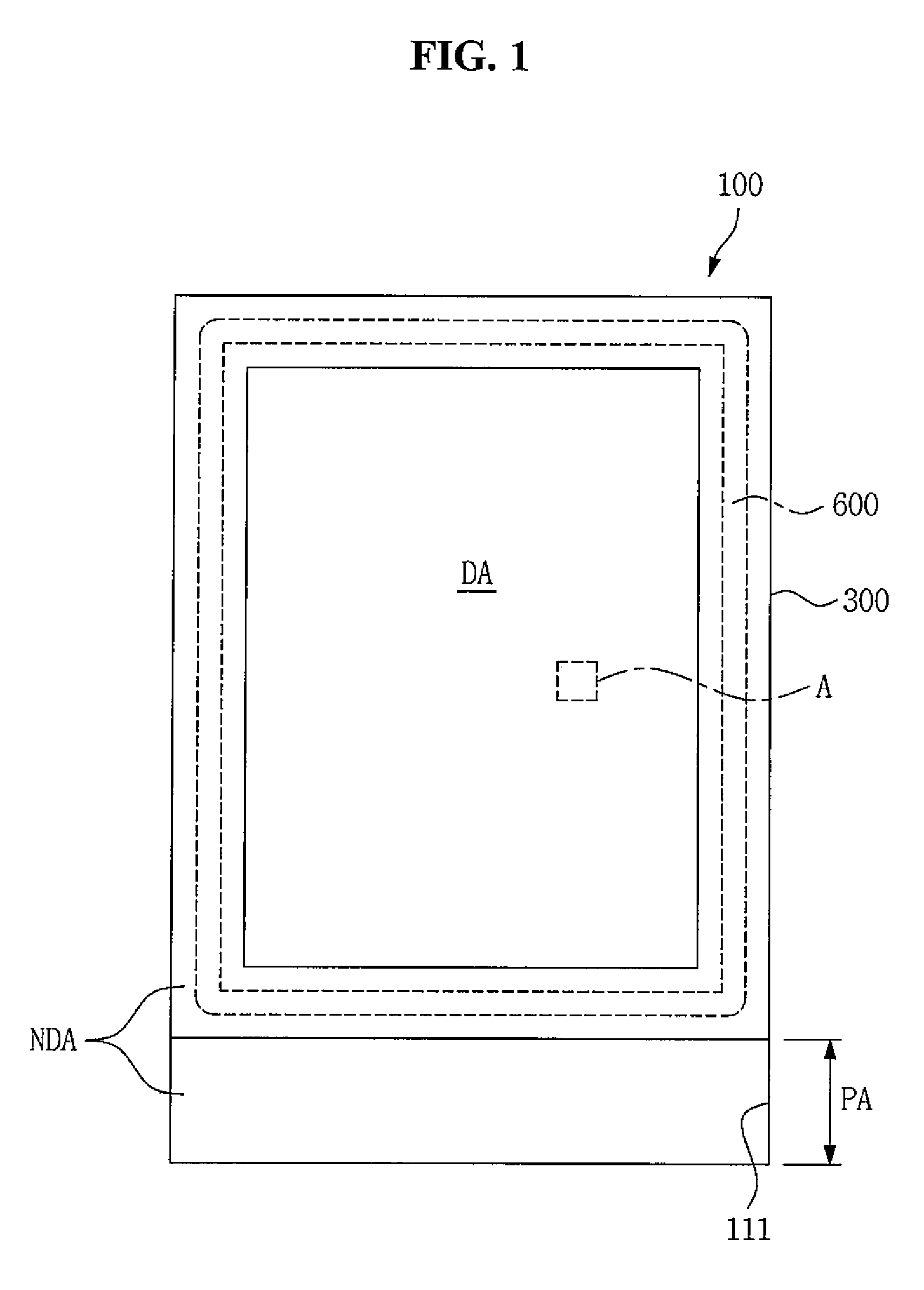
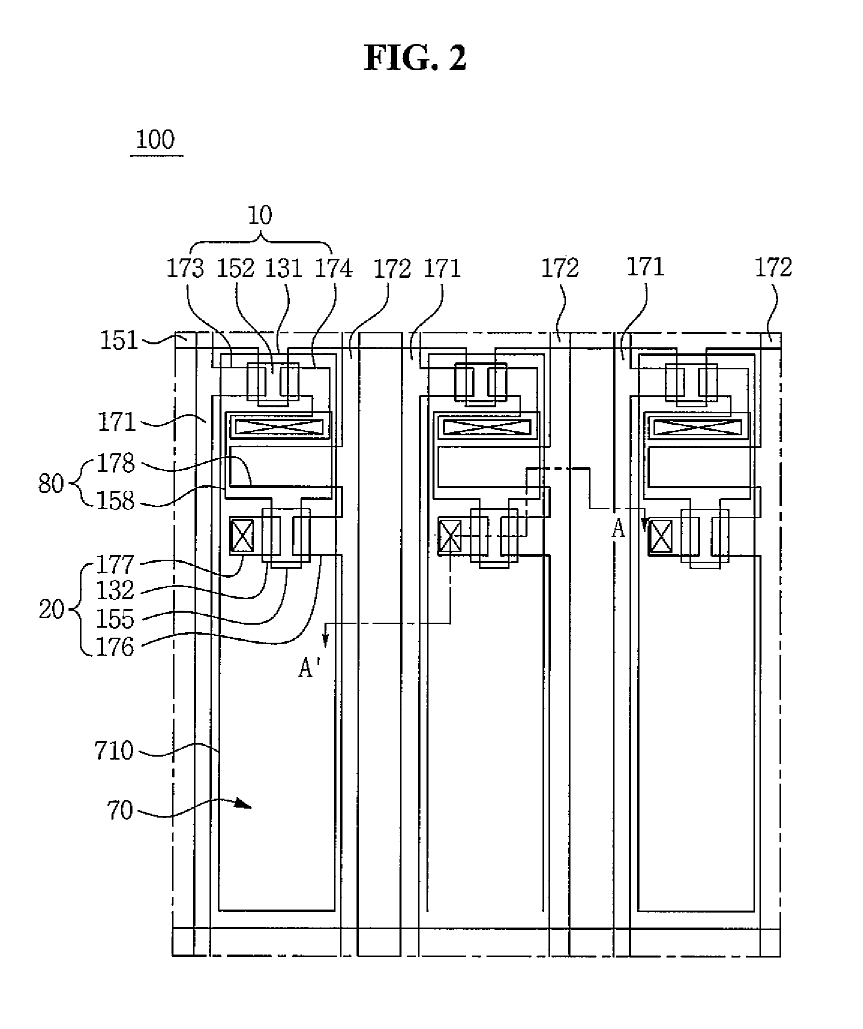
[0044]Aspects and features of the present invention and methods for achieving them will be made clear from example embodiments described below in detail with reference to the accompanying drawings. Aspects of the present invention may, however, be embodied in many different forms and should not be construed as being limited to the example embodiments set forth herein. Rather, these embodiments are provided so that this disclosure will be thorough and complete, and will fully convey the spirit and scope of the present invention to those skilled in the art. The present invention is defined by the spirit and scope of the claims, and their equivalents. Therefore, well-known constituent elements, operations, and techniques may not be described in detail in the example embodiments, in order to prevent the present invention from being obscurely interpreted. Like reference numerals refer to like elements throughout the specification.

[0045]The spatially relative terms “below”, “beneath”, “lo...


PUM


Abstract

A display device includes: a substrate; a pixel defining layer defining a pixel region on the substrate; a first electrode on the pixel region; a light emitting layer on the first electrode; a second electrode on the light emitting layer; a thin film encapsulation layer on the second electrode; a metal pattern on the thin film encapsulation layer and overlapping the pixel defining layer; and a multi-layer thin film layer on the metal pattern and the thin film encapsulation layer.

Description

CROSS-REFERENCE TO RELATED APPLICATION[0001]This application claims priority to and the benefit of Korean Patent Application No. 10-2014-0105807, filed on Aug. 14, 2014, with the Korean Intellectual Property Office, the disclosure of which is incorporated herein in its entirety by reference.BACKGROUND[0002]1. Field[0003]Aspects of some embodiments of the present invention relate to a display device, and to a method of manufacturing the display device.[0004]2. Description of the Related Art[0005]In general, flat panel display devices (such as a liquid crystal display device or an organic light emitting display device) includes a plurality of pairs of electrodes for generating an electric field, and an electro-optical active layer interposed therebetween. The liquid crystal display device includes a liquid crystal layer as the electro-optical active layer. An organic light emitting diode (OLED) of the organic light emitting display device includes an organic light emitting layer as th...

Claims


Application Information

Patent Timeline
Patent Type & Authority Patents(United States)
IPC IPC(8): H01L27/02H01L27/15H01L33/54
CPCH01L27/156H01L33/54H01L2933/005G02F1/133509H10K59/12H10K50/8445H10K50/86H10K50/865H10K59/1201H10K71/621H10K71/00
Inventor KIM, SOO YOUNKIM, HYUN HOKIM, SEUNG HUNCHO, SANG HWAN
Owner SAMSUNG DISPLAY CO LTD
Why Eureka
Try Eureka