
Terminal plate circuit

a terminal plate and circuit technology, applied in the direction of substation/switching arrangement details, electrical equipment, cooling/ventilation/heating modifications, etc., can solve the problems of diode heat generation violently, temperature of diode may exceed the proper operating temperature of diode, diode failure to function, etc., to achieve the effect of large heat dissipation effect of diod

Inactive Publication Date: 2015-11-24
ONAMBA CO LTD
View PDF18 Cites 0 Cited by
  • Summary
  • Abstract
  • Description
  • Claims
  • Application Information

AI Technical Summary

Benefits of technology

The present invention is a terminal plate circuit that helps to efficiently transmitting heat from a diode to the terminal plate through solder. It achieves this by allowing air bubbles to escape from the diode to the outside through streaks formed on the surface of the terminal plate. This results in a large effect of heat dissipation from the diode, making it highly suitable for use in severe environments such as terminal boxes for solar cell panels.

Problems solved by technology

When the diode performs the aforementioned function, a large electric current flows in the forward direction of the diode, so that the diode generates heat violently, and the temperature thereof may exceed a proper operating temperature of the diode.
In such cases, not only will the diode fail to function as a diode (heat burst) but also the diode and the surrounding circuit may have a fear of being broken.
Further, even if they are not broken, the life of the diode will be extremely shortened when such a heat burst is repeated.
Therefore, the generated heat must be efficiently dissipated so that the heat generated during the operation of the diode may not exceed a proper operating temperature of the diode.
However, when the bottom surface of the diode is soldered and attached to the surface of the enlarged terminal plate, air bubbles are mixed into the solder during the soldering, and the air bubbles lower the efficiency of heat transfer from the diode to the terminal plate, whereby the heat of the diode is not efficiently dissipated.

Method used


Image

  • Terminal plate circuit
  • Terminal plate circuit
  • Terminal plate circuit

Examples


examples

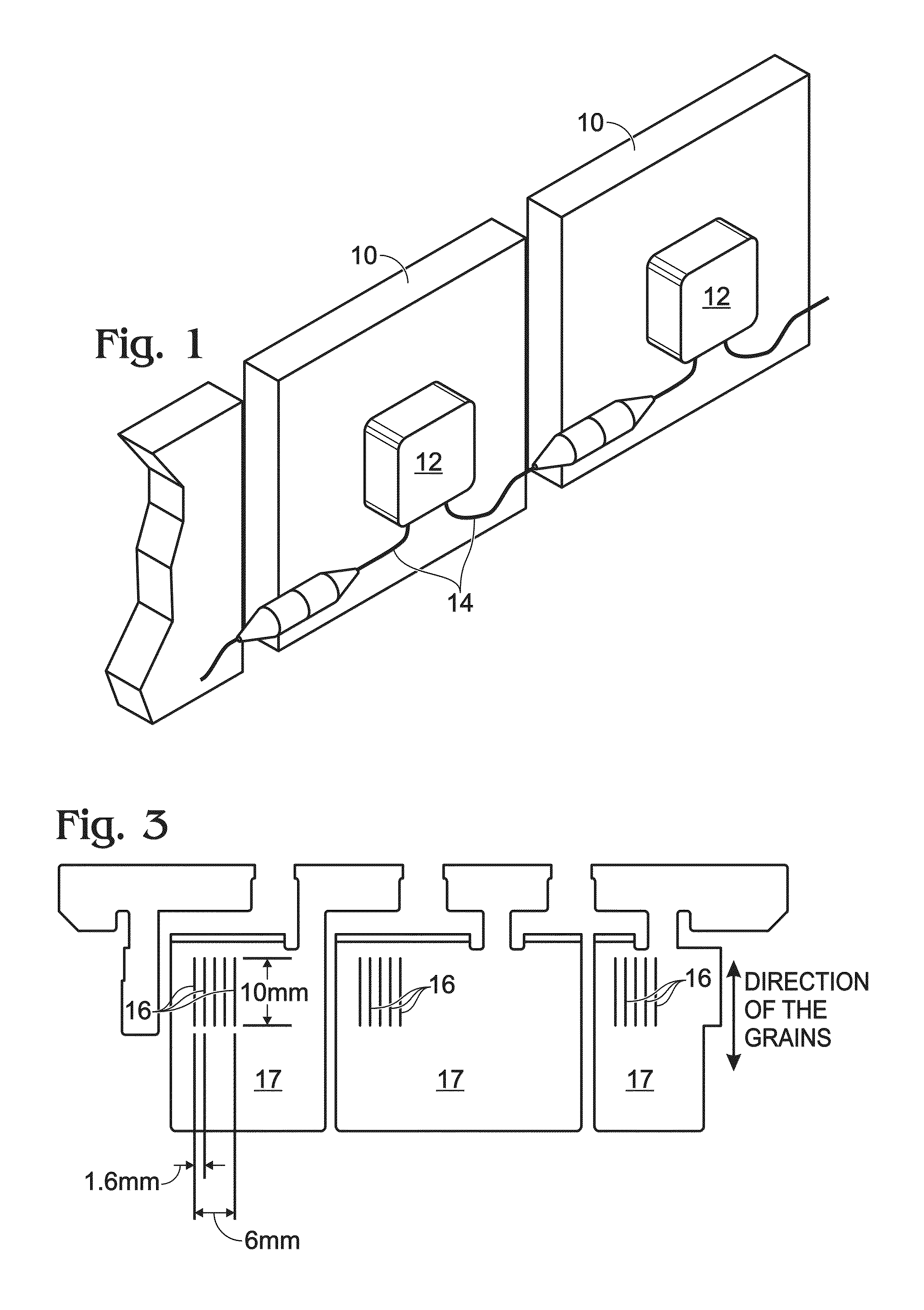
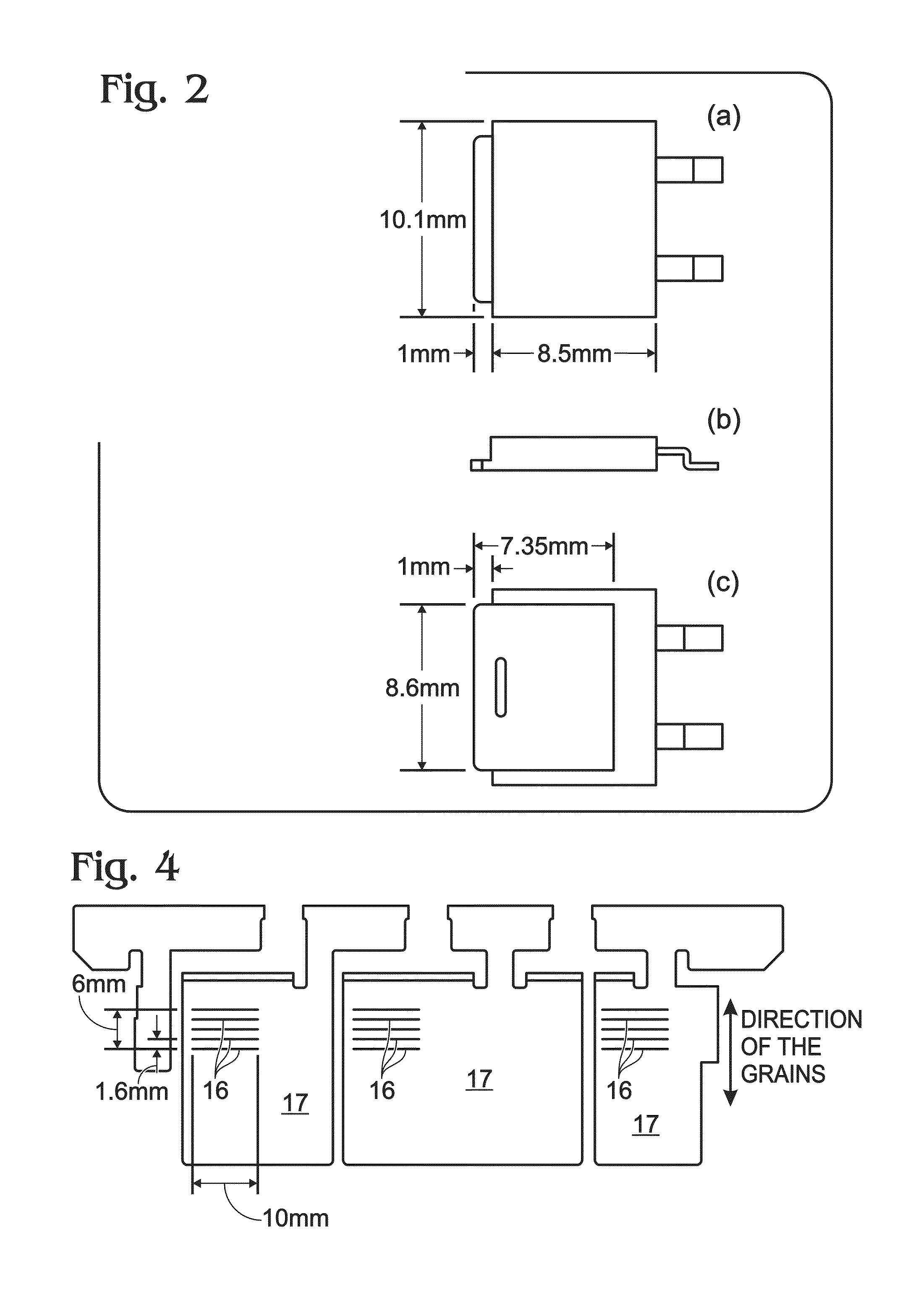
[0026]Terminal plates having grains 17 and streaks 16 consisting of a plurality of straight lines that are parallel to the grains as shown in FIG. 3, terminal plates having grains 17 and streaks 16 consisting of a plurality of straight lines that are perpendicular to the grains as shown in FIG. 4, terminal plates having grains 17 and grid-like streaks 16 that are formed by intersections of a plurality of straight lines that are parallel to the grains 17 and a plurality of straight lines that are perpendicular to the grains as shown in FIG. 5, and terminal plates having a configuration similar to that of FIG. 3 having grains 17 but without having streaks were respectively prepared in triplicate, and a metal part of a bottom surface of a diode of surface mounting type shown in FIG. 2 was soldered onto the surface of each terminal plate. Then, a photograph was taken with an X-ray (90 kV, 90 mA) from above the diode, and a state of generation of air bubbles within the solder was confirm...


PUM


Abstract

In a terminal plate circuit in which the bottom surface of the diode is attached to the surface of the terminal plate with solder so as to dissipate the heat of the diode, heat transfer from the diode to the terminal plate is facilitated by removing the air bubbles in the solder during the soldering. A terminal plate circuit configured in such a manner that a metal part of a bottom surface of a diode of surface mounting type is soldered onto a surface of a terminal plate that is larger than the metal part, characterized in that streaks consisting of a plurality of lines that do not intersect with each other are formed on the surface of the terminal plate onto which the diode is to be soldered, whereby air bubbles generated within the solder during the soldering are let to escape from a lower surface of the diode to outside through the streaks. This terminal plate circuit is suitable for the use in a terminal box for solar cell panel.

Description

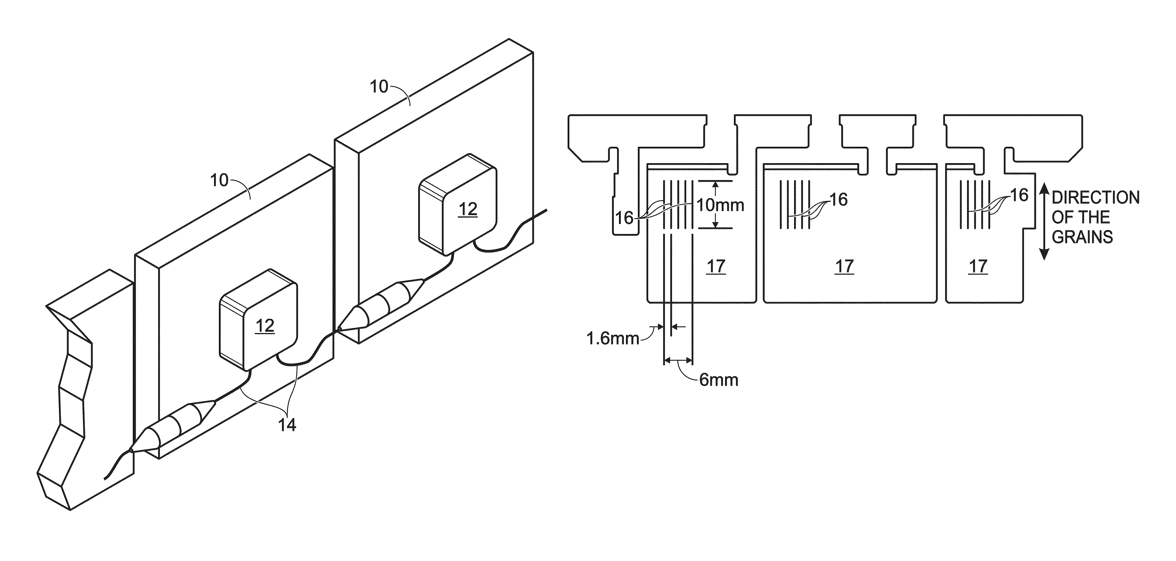
TECHNICAL FIELD OF THE INVENTION[0001]The present invention relates to a terminal plate circuit that is used in a severe environment such as in a terminal box for solar cell panel.BACKGROUND ART[0002]Description will be made by using as an example a terminal plate circuit within terminal boxes for solar cell panel that are arranged in a large number on a roof of a house or the like. FIG. 1 shows a schematic view of a rear surface of a solar cell panel. As is clear from FIG. 1, each solar cell panel 10 has a terminal box 12 mounted on a rear surface thereof. Terminal boxes 12 of adjacent solar cell panels 10 are electrically connected with each other via an external connection cable 14.[0003]In the inside of the terminal box, a pair of terminal plates are mounted, one end thereof is connected to the external connection cable, and the other end thereof is connected to the electrode of the solar cell panel. Further, a diode is incorporated in the inside of the terminal box so as to con...

Claims


Application Information

Patent Timeline
IPC IPC(8): H02B1/01H02B1/56H05K7/20H02S40/34
CPCH02S40/345Y02E10/50H02B1/01
Inventor ISHIDA, JUNHAMANO, KENJI
Owner ONAMBA CO LTD
Learn More