
Method and system for providing a smart memory architecture

a memory architecture and resistive type technology, applied in the field of smart memory architecture, can solve the problems of not being designed for, or applied specifically to, memory with high error rate and probabilistic tendencies, not all memory cells on a memory chip functioning properly, etc., and achieves the effects of slow read/write times, high error rates, and high error rates

Active Publication Date: 2015-06-30
SAMSUNG ELECTRONICS CO LTD
View PDF20 Cites 13 Cited by
  • Summary
  • Abstract
  • Description
  • Claims
  • Application Information

AI Technical Summary

Benefits of technology

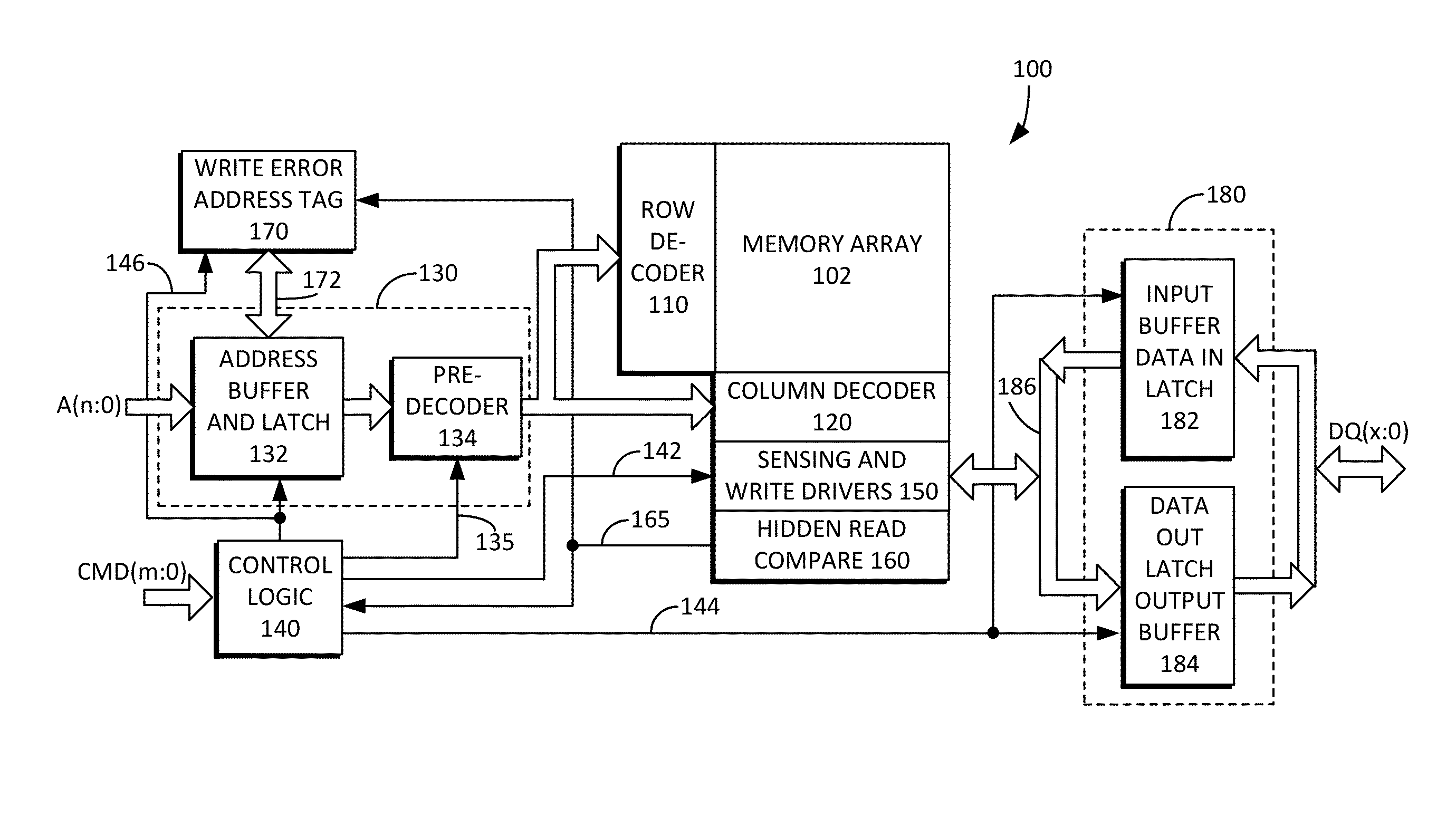
The inventive concepts described in this patent text make a smart memory system that can work seamlessly with memories that have high error rates and slow read / write times relative to a logic processor. The system can reliably use non-volatile memory bits by tagging the failed location and corresponding data, and by performing re-writes at a convenient time or simply masking the failed location and re-writing the data to a different location. The system also incorporates a common asynchronous memory bus with acknowledgement signaling to guarantee write and read success, and a handshaking memory interface that allows for process-independent, voltage-independent, and temperature-independent operation by using internal read and write tracking and verifying schemes.

Problems solved by technology

Unfortunately, with STT-RAM or any other type of memory chip, manufacturing or other defects may result in not all memory cells on a memory chip functioning properly.
Memory repair is not made available to the memory's end-user.
Although these and other systems have addressed similar problems to those addressed by the present inventive principles, they have not been designed for, or applied specifically to, memory with high error rates and probabilistic tendencies such as PCRAM, MRAM, and RRAM devices.

Method used


Image

  • Method and system for providing a smart memory architecture
  • Method and system for providing a smart memory architecture
  • Method and system for providing a smart memory architecture

Examples


Embodiment Construction

[0087]Reference will now be made in detail to embodiments of the inventive concept, examples of which are illustrated in the accompanying drawings. In the following detailed description, numerous specific details are set forth to enable a thorough understanding of the inventive concept. It should be understood, however, that persons having ordinary skill in the art may practice the inventive concept without these specific details. In other instances, well-known methods, procedures, components, circuits, and networks have not been described in detail so as not to unnecessarily obscure aspects of the embodiments.

[0088]It will be understood that, although the terms first, second, etc. may be used herein to describe various elements, these elements should not be limited by these terms. These terms are only used to distinguish one element from another. For example, a first circuit could be termed a second circuit, and, similarly, a second circuit could be termed a first circuit, without ...


PUM


Abstract

A smart memory system preferably includes a memory including one or more memory chips, and a processor including one or more memory processor chips. The processor may include a common address / data / control memory bus that is configured to provide an asynchronous handshaking interface between the memory array and the memory processor. The processor can offload error data from the memory chip for analysis, and can store poor retention bit address information for memory refreshing in a non-volatile error retention memory. Program logic can also be included for memory address re-configuration. Power management logic can also be included, which may have a process-voltage-temperature compensation voltage generator for providing stable and constant read currents. An asynchronous handshaking interface is provided between the memory array and the memory processor. Write error tagging and write verification circuits can also be included.

Description

CROSS-REFERENCES TO RELATED APPLICATIONS[0001]This application claims the benefit of commonly assigned provisional application Ser. No. 61 / 597,773, filed Feb. 11, 2012, entitled “A METHOD AND SYSTEM FOR PROVIDING A SMART MEMORY ARCHITECTURE,” the contents of which is incorporated herein by reference in its entirety.BACKGROUND[0002]The present inventive concepts relate to a smart memory architecture, and more particularly to a method and system for providing a smart memory architecture for resistive type memory.[0003]The present inventive concepts relate to memory systems for storing and retrieving information from memory integrated circuits, including static random access memory (SRAM), dynamic random access memory (DRAM), Flash memory, phase-change random access memory (PCRAM), spin-transfer torque random access memory (STT-RAM), magnetic random access memory (MRAM), resistive random access memory (RRAM), and future memory devices. Inventive aspects described herein are particularl...

Claims


Application Information

Patent Timeline
Patent Type & Authority Patents(United States)
IPC IPC(8): G06F11/00G06F15/167G06F11/10G06F3/06G06F11/07G06F12/00G11C11/16G06F21/00G11C13/00
CPCG06F15/167G06F11/1076G06F11/1008G06F3/0601G06F11/0751G06F11/0793G06F12/00G11C11/16G06F21/00G11C13/0002G11C11/1677G11C11/1695G11C29/00
Inventor ONG, ADRIAN
Owner SAMSUNG ELECTRONICS CO LTD
Learn More