
Electronic device comprising RF-LDMOS transistor having improved ruggedness

a technology of rfldmos and transistor, which is applied in the direction of pulse manipulation, emergency protective arrangements for limiting excess voltage/current, pulse technique, etc., can solve the problem of low power dissipation of the rectifying element, and achieve the effect of improving rf ruggedness and compromising the rf performance of the rf-ldmos

Inactive Publication Date: 2015-04-28
AMPLEON NETHERLANDS
View PDF7 Cites 2 Cited by
  • Summary
  • Abstract
  • Description
  • Claims
  • Application Information

AI Technical Summary

Benefits of technology

The invention is about a new electronic device that is more robust and reliable than existing devices. The electronic device includes a RF-LDMOS transistor and a clipping circuit that helps keep the voltage on the clipping node below a predefined reference voltage. This prevents the voltage on the clipping node from affecting the performance of the RF-LDMOS transistor during normal operation or a ruggedness event. The electronic device also includes a small rectifying element that can handle large amounts of current with low power dissipation. This results in better performance and smaller size of the electronic device, which is beneficial for parasitic capacitances. The invention also provides a power amplifier and an integrated multi-stage power amplifier module with improved ruggedness. Additionally, the invention can be used in a cellular base station for better performance and reliability.

Problems solved by technology

This results in low power dissipation in the rectifying element, in particular when a diode or a series of diodes is used, because of the low voltage drop over the rectifying element (diode).

Method used


Image

  • Electronic device comprising RF-LDMOS transistor having improved ruggedness
  • Electronic device comprising RF-LDMOS transistor having improved ruggedness
  • Electronic device comprising RF-LDMOS transistor having improved ruggedness

Examples


first embodiment

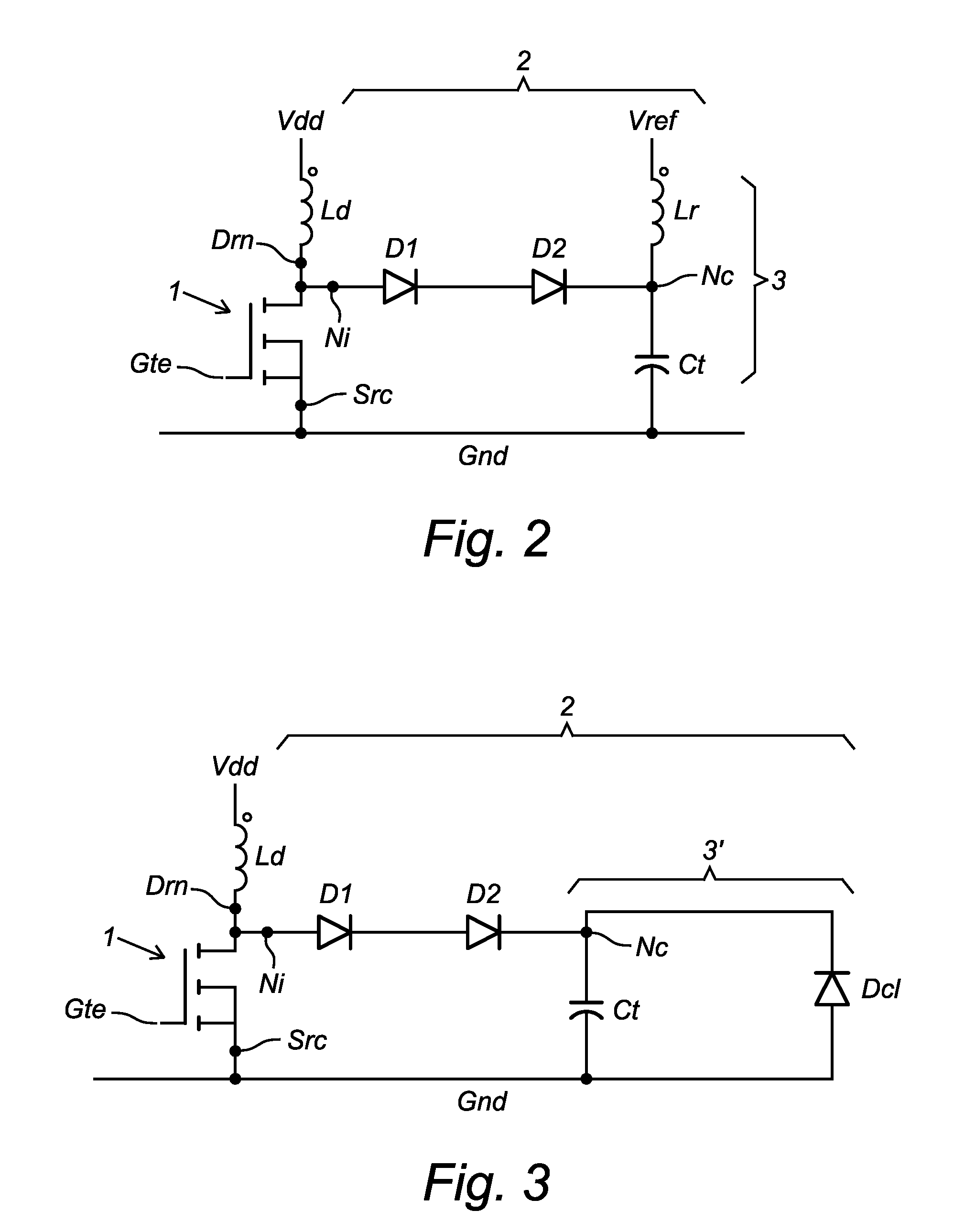
[0102]FIG. 2 shows an equivalent circuit diagram of an electronic device in accordance with the invention. On the left side of FIG. 2 there is shown the RF-LDMOS transistor 1 which is connected, via a drain terminal bondwire Ld (with an inductance), with its drain terminal Drn to a drain lead connected to a power supply voltage Vdd. This supply voltage Vdd is typically within the range of 28V to 50V. An LDMOS device optimized for 28V will have slightly other dimensions then the 50V variant. The RF-LDMOS transistor also comprises a gate terminal Gte which is typically connected to a gate lead via a further bondwire (not shown). The source terminal Src of the LDMOS transistor 1 is connected to the ground voltage (potential) Gnd. As already mentioned the source terminal of the RF-LDMOS is typically at the backside of a substrate. Typically, the substrate onto which the RF-LDMOS is manufactured is directly provided on and in electrical contact with a source lead.

[0103]The electronic dev...

second embodiment

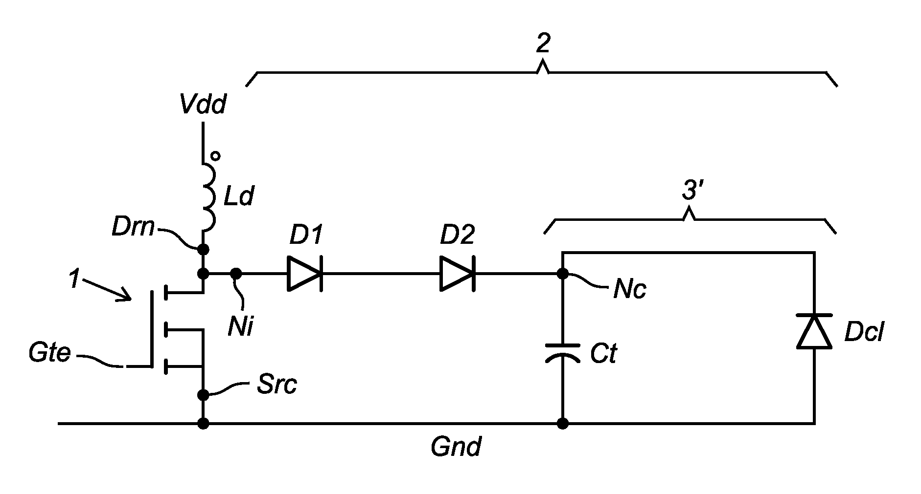
[0109]FIG. 3 shows an equivalent circuit diagram of an electronic device in accordance with the invention. This embodiment will be discussed in as far as it differs from FIG. 2. Sometimes, it may be inconvenient to feed the extra reference voltage Vref via additional bondwires to the chip. In the embodiment of FIG. 3 the reference voltage is created on the die itself. The main difference between FIG. 3 and FIG. 2 is that in FIG. 3 there is an alternative clipping circuit 3′. The alternative clipping circuit 3′ comprises the capacitance Ct and a clipping diode Dcl connected in parallel with the capacitance Ct, wherein the anode side of the clipping diode Dcl is connected to the ground voltage (further reference voltage terminal), i.e. in normal operation the clipping diode Dcl is reverse-biased.

[0110]A clipping diode Dcl with a breakdown voltage equal to the earlier mentioned reference voltage Vref in FIG. 2, is integrated near to capacitance Ct. This clipping diode Dcl must be able ...


PUM


Abstract

The invention relates to an electronic device comprising an RF-LDMOS transistor (1) and a protection circuit (2) for the RF-LDMOS transistor. The protection circuit (2) comprises: i) an input terminal (Ni) coupled to a drain terminal (Drn) of the RF-LDMOS transistor (1); ii) a clipping node (Nc); iii) a clipping circuit (3) coupled to the clipping node (Nc) for substantially keeping the voltage on the clipping node (Nc) below a predefined reference voltage, wherein the predefined reference voltage is designed to be larger than the operation voltage on the drain terminal (Drn) and lower than a trigger voltage of a parasitic bipolar transistor (100) that is inherently present in the RF-LDMOS transistor; iv) a capacitance (Ct) coupled between the clipping node (Nc) and a further reference voltage terminal (Gnd), and v) a rectifying element (D1, D2) connected with its anode terminal to the input terminal (Ni) and with its cathode terminal to the clipping node (Nc). The invention provides an RF-LDMOS transistor having an improved RF ruggedness, while not, or at least to a much lesser extent, compromising the RF performance of the RF-LDMOS transistor.

Description

CROSS-REFERENCE TO RELATED APPLICATIONS[0001]This application claims the priority under 35 U.S.C. §119 of European patent application no. 12167901.3, filed on May 14, 2012, the contents of which are incorporated by reference herein.FIELD OF THE INVENTION[0002]The invention relates to an electronic device comprising an RF-LDMOS transistor and a protection circuit for the RF-LDMOS transistor.BACKGROUND ART[0003]In base stations for personal communication systems (GSM, EDGE, W-CDMA), RF-power amplifiers (PA) are key components. For these power amplifiers, RF Laterally Diffused MOS (LDMOS) transistors are the standard choice of technology, because of their excellent power capabilities gain, linearity and reliability.[0004]An RF power amplifier is a type of electronic amplifier used to convert a low-power radio-frequency signal into a larger signal of significant power, typically for driving the antenna of a transmitter. It is usually optimized to have high efficiency, high output Power ...

Claims


Application Information

Patent Timeline
Patent Type & Authority Patents(United States)
IPC IPC(8): H01L29/78H03G11/02H03K17/0814
CPCH01L29/7818H03G11/02H03K17/08142
Inventor DE BOET, JOHANNES ADRIANUS MARIA
Owner AMPLEON NETHERLANDS
Learn More