Coil-type electronic component
a technology of electronic components and coils, applied in the direction of transformers/inductances, magnetic cores, magnetic bodies, etc., can solve the problem that the reduction of further size cannot be fully supported, and achieve the effect of high specific resistance, low magnetic loss, and high magnetic characteristics
- Summary
- Abstract
- Description
- Claims
- Application Information
AI Technical Summary
Benefits of technology
Problems solved by technology
Method used
Image
Examples
example 1
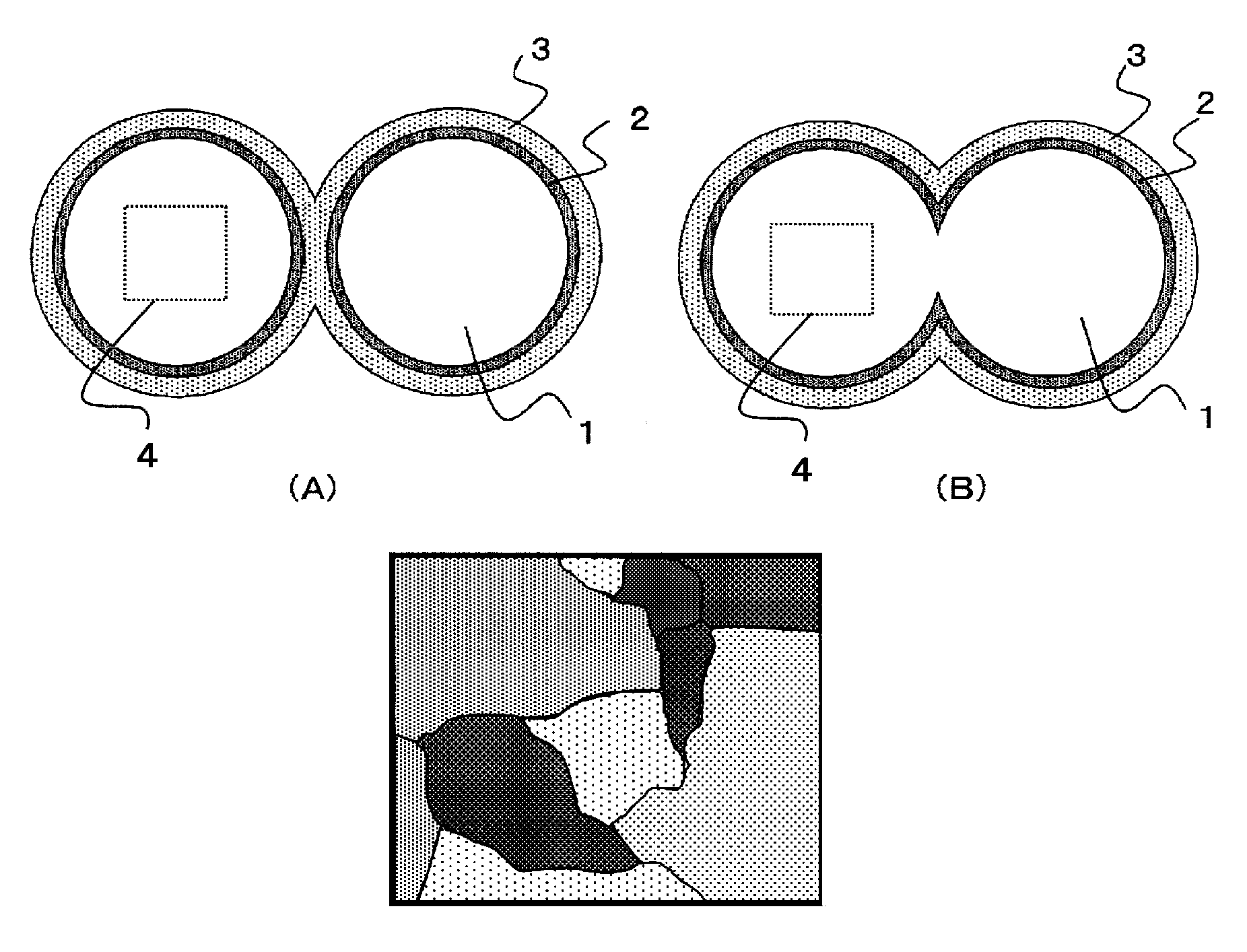
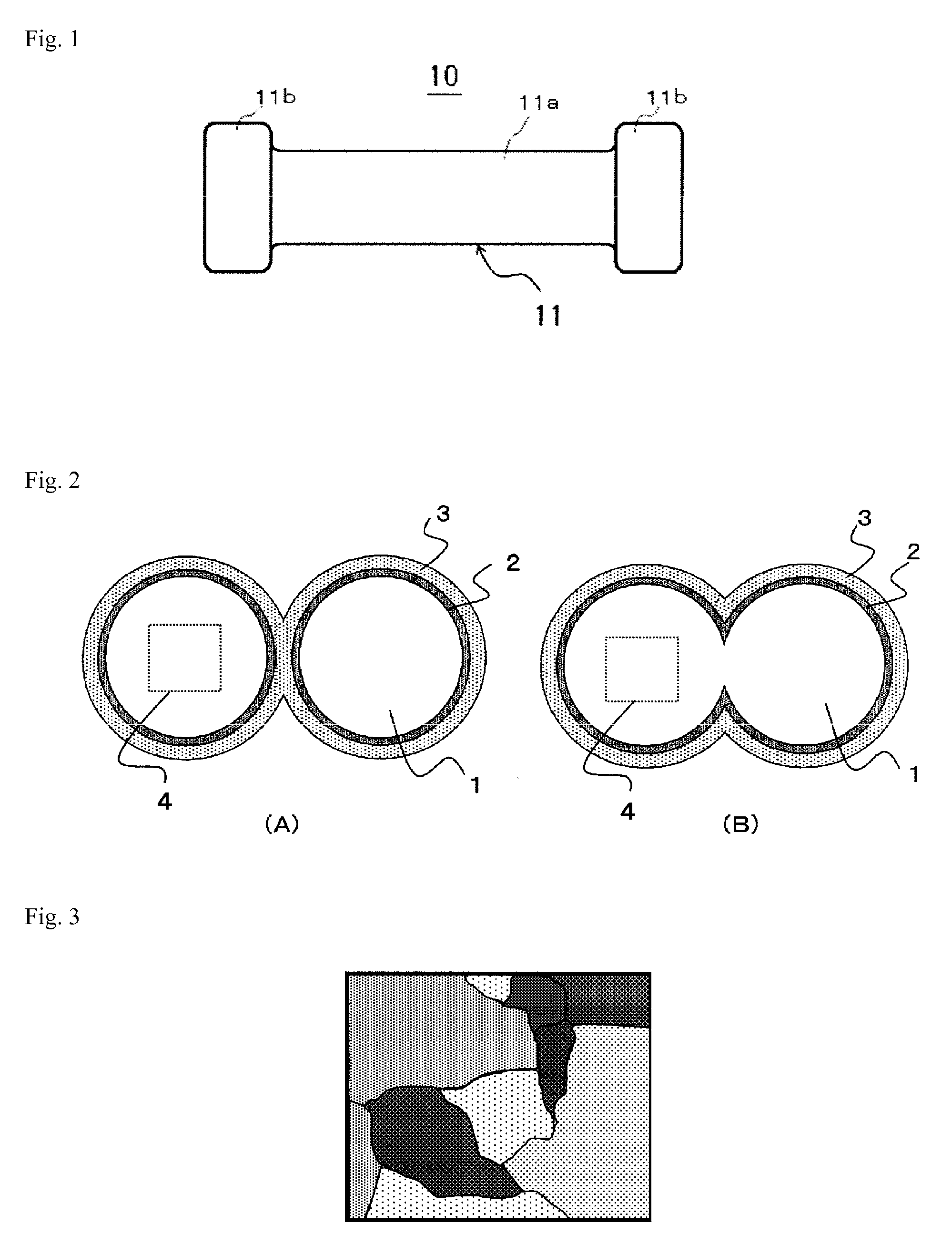
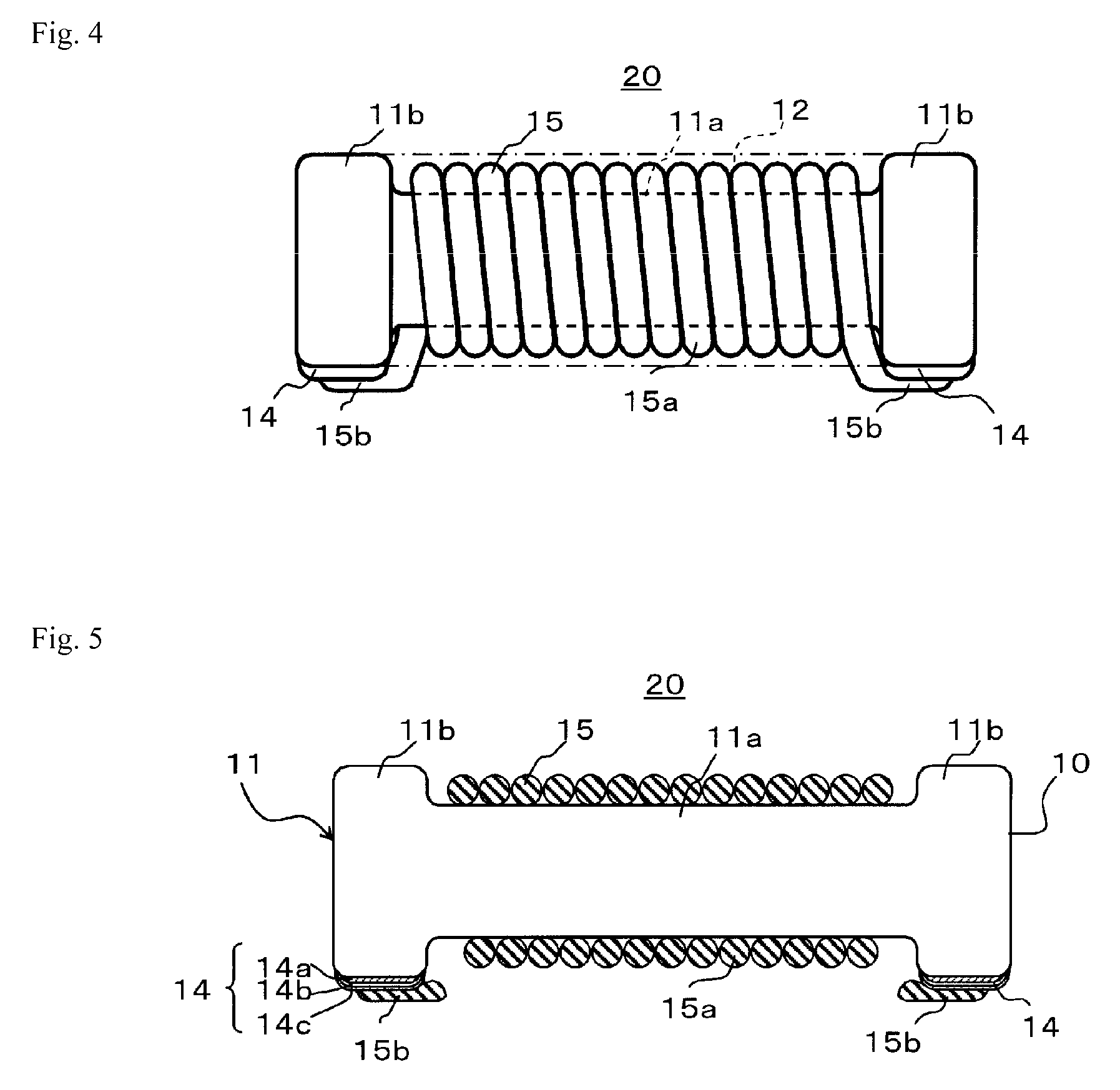
[0131]For the material grains to obtain a base material using a soft magnetic alloy for an electronic component, alloy powder (PF-20F manufactured by Epson Atmix K.K.) was used which is a type of water-atomized powder whose average grain size (d50%) is 10μ and composition ratio was 5 percent by weight of chromium, 3 percent by weight of silicon and 92 percent by weight of iron. The average grain size d50% of material grains described above was measured using a granularity analyzer (9320HRA manufactured by Nikkiso). Each of the above grains was polished until its cross-section in a thickness direction cutting across roughly the center of the grain was exposed, and the obtained cross-section was captured with a scanning electron microscope (SEM: S-4300SE / N manufactured by Hitachi High-Technologies) at a magnification of 3000 times to obtain a composition image, which was then used to calculate the composition near the center of the grain and also near the surface by the ZAF method thr...
example 2
[0141]An evaluation sample was prepared in the same manner as in Example 1, except that the composition ratio of the material grain was changed to 3 percent by weight of chromium, 5 percent by weight of silicate, and 92 percent by weight of iron. The obtained results are shown in Table 1.
[0142]As shown in Table 1, good measurement results were obtained, just as in Example 1, such as 53 in magnetic permeability μ, 9 kgf / mm2 in base material strength (rupture stress), 2.0×10⁷ Ω·cm in volume resistivity, and 1.1×10⁷ W / m3 in magnetic loss Pcv.
[0143]FE-SEM observation, SEM observation, and SEM-EDS analysis, performed in the same manner as in Example 1, also confirmed that in-grain crystal grains had formed due to heat treatment, and a metal oxide (oxide layer) had also formed on the grain surface, where the formed oxide layer had a two-layer structure constituted by an inner layer 2 (average thickness: 30 nm) formed by chromium oxide and an outer layer 3 (average thickness: 66 nm) formed...
example 3
[0144]An evaluation sample was prepared in the same manner as in Example 1, except that the composition ratio of the material grain was changed to 6 percent by weight of chromium, 2 percent by weight of silicate, and 92 percent by weight of iron. The obtained results are shown in Table 1.
[0145]As shown in Table 1, good measurement results were obtained, just as in Example 1, such as 49 in magnetic permeability μ, 14 kgf / mm2 in base material strength (rupture stress), 7.0×10⁶ Ω·cm in volume resistivity, and 2.0×10⁷ W / m3 in magnetic loss Pcv.
[0146]FE-SEM observation, SEM observation, and SEM-EDS analysis, performed in the same manner as in Example 1, also confirmed that in-grain crystal grains had formed due to heat treatment, and a metal oxide (oxide layer) had also formed on the grain surface, where the formed oxide layer had a two-layer structure constituted by an inner layer 2 (average thickness: 50 nm) formed by chromium oxide and an outer layer 3 (average thickness: 80 nm) forme...
PUM
| Property | Measurement | Unit |
|---|---|---|
| temperature | aaaaa | aaaaa |
| grain size d50 | aaaaa | aaaaa |
| temperature | aaaaa | aaaaa |
Abstract
Description
Claims
Application Information
 - R&D
- Intellectual Property
- Life Sciences
- Materials
- Tech Scout
- Unparalleled Data Quality
- Higher Quality Content
- 60% Fewer Hallucinations
Browse by: Latest US Patents, China's latest patents, Technical Efficacy Thesaurus, Application Domain, Technology Topic, Popular Technical Reports.
© 2025 PatSnap. All rights reserved.Legal|Privacy policy|Modern Slavery Act Transparency Statement|Sitemap|About US| Contact US: help@patsnap.com


