
Printed wiring board, build-up multi-layer board, and production method therefor

a printing board and multi-layer technology, applied in the direction of printed circuit, cable/conductor manufacturing, metal adhesion improvement of the insulation substrate, etc., can solve the problems of reduced resin amount, complicated soft etching treatment steps, and reduced resin amount, etc., to achieve excellent connection reliability and reduce resin amount

Inactive Publication Date: 2014-10-21
PANASONIC CORP
View PDF18 Cites 0 Cited by
  • Summary
  • Abstract
  • Description
  • Claims
  • Application Information

AI Technical Summary

Benefits of technology

[0011]According to the printed wiring board of the present invention, by laminating a plurality of pores provided between the plurality of insulating layers on the same plane as that of the wiring patterns, occurrence of internal structural defects such as delamination can be suppressed, so that defects such as swelling does not occur during reflow. Furthermore, by providing a plurality of pores on the surface layer, adhesion of the resist, the plated conductor, and the like, can be improved, thus enabling finer wiring. Thus, a multilayer printed wiring board free from structural defects such as delamination can be provided. At the same time, by forming a plurality of pores in the portion surrounding the plated conductor on the insulating layer, or by providing a plurality of protrusions as an anchor at the insulating layer side of the plated conductor, it is possible to provide a multi-layer printed wiring board having excellent connection reliability in which occurrence of cracks due to the difference in the thermal expansion coefficients in the through hole and via hole portions.

Problems solved by technology

Furthermore, the amount of resin is being reduced because of thinning of the insulating layer according to the miniaturization, and as a result, delamination occurs due to shortage of the adhesion force of the inner layer.
Furthermore, steps of soft etching treatment may be complicated.
However, this method may be insufficient to correspond to fine patterning.
Furthermore, when a plated conductor is thinned for forming a fine pattern and the density of the wiring is further increased, during heating or in heat cycle conditions, in through holes and via holes, disconnection caused by cracks due to a difference in the thermal expansion coefficients between these members, peeling with respect to the insulating layer and the plated conductor, and the like, occur.
As a result, sufficient connection reliability cannot be secured.

Method used


Image

  • Printed wiring board, build-up multi-layer board, and production method therefor
  • Printed wiring board, build-up multi-layer board, and production method therefor
  • Printed wiring board, build-up multi-layer board, and production method therefor

Examples


first exemplary embodiment

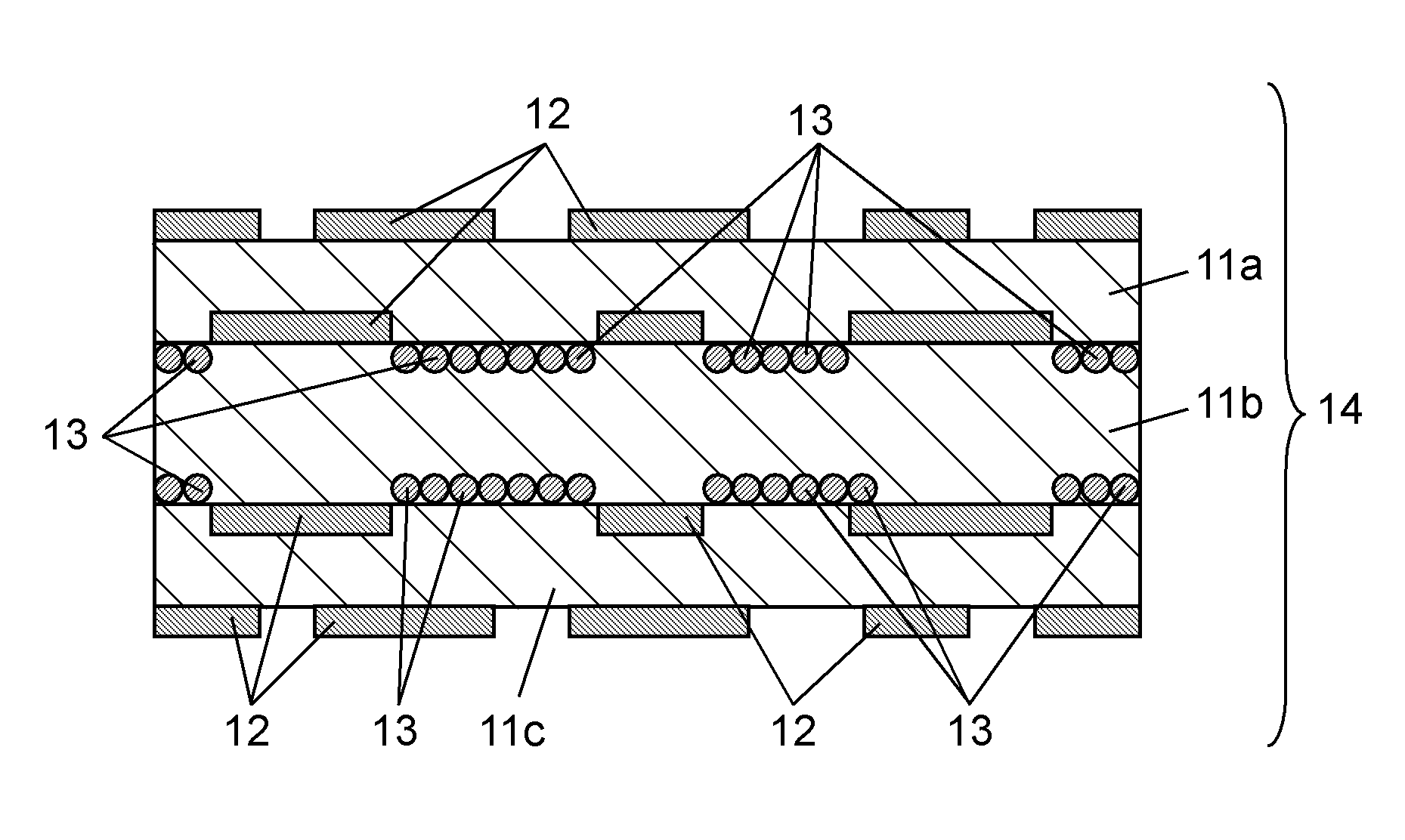
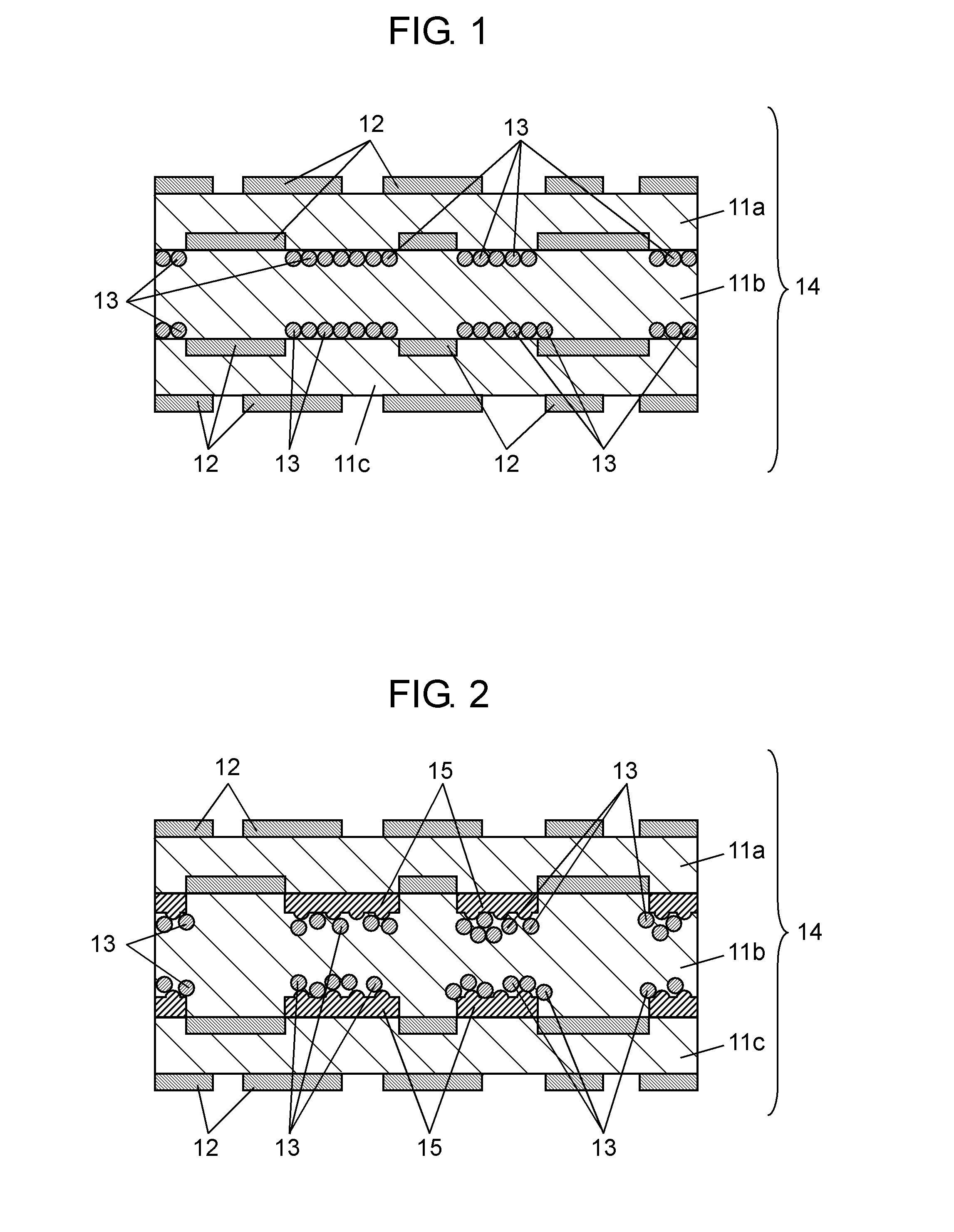
[0052]Hereinafter, a printed wiring board in accordance with a first exemplary embodiment of the present invention is described. FIG. 1 is a sectional view showing an example of a structure of the printed wiring board in accordance with the first exemplary embodiment of the present invention.

[0053]Insulating layers 11a, 11b, and 11c, wiring patterns 12, pores 13, and printed wiring board 14 are shown in FIG. 1.

[0054]Printed wiring board 14 shown in FIG. 1 includes a plurality of insulating layers 11a, 11b, and 11c, a plurality of wiring patterns 12 obtained by etching copper foil into predetermined patterns, and a plurality of pores 13 provided between wiring patterns 12. In FIG. 1, pores 13 are provided in all of the portions between wiring patterns 12, but may be provided in at least a part of the portions between wiring patterns 12.

[0055]Insulating layers 11a, 11b and 11c of printed wiring board 14 include at least resin, glass woven fabric and / or nonwoven fabric, inorganic fille...

second exemplary embodiment

[0114]Next, as a second exemplary embodiment, improvement of adhesion of resist to be provided on the outermost layer of printed wiring board 14 is described.

[0115]FIG. 6 is a sectional view showing an example of a structure of a printed wiring board in which resists are provided on the outermost layers. Resists 19, for example, photo-sensitive solder resists are shown in FIG. 6. In FIG. 6, a part of resists 19 may be provided such that they cover wiring pattern 12 provided on the outermost layers of printed wiring board 14 (this case is not shown).

[0116]In printed wiring board 14 shown in FIG. 6, a plurality of insulating layers 11a, 11b and 11c are laminated by way of a plurality of pores 13, resin-filled layer 15 (not shown in FIG. 6) or the like provided adjacent to incorporated wiring patterns 12.

[0117]As shown in FIG. 6, a plurality of pores 13 are provided on insulating layers 11a and 11c expressed to the outermost layers of printed wiring board 14 (or between wiring patterns...

third exemplary embodiment

[0121]Next, application to a printed wiring board having a build-up layer is described with reference to FIG. 8.

[0122]FIG. 8 is a sectional view illustrating the improvement of an adhesion force of a plated conductor in a printed wiring board having the build-up layer.

[0123]Build-up layer 20, and plated conductor 21 are shown in FIG. 8. Plated conductor 21 provided in build-up layer 20 is formed of, for example, copper wiring, copper via holes, or the like, by using plating techniques such as copper plating.

[0124]When plated conductor 21 is used for a surface layer and the like if necessary, a via electrode formed on build-up layer 20 (the via electrode corresponds to an interlayer connection portion between a plurality of wiring) or wiring (the wiring corresponds to wiring patterns 12 formed by plating on the surface layer or the inner layer of build-up layer 20) can be formed finely and densely.

[0125]Note here that build-up layer 20 is not necessarily allowed to contain glass wove...


PUM

PropertyMeasurementUnit
temperatureaaaaaaaaaa
volume fractionaaaaaaaaaa
dielectric constantaaaaaaaaaa

Abstract

A multi-layer printed-wiring-board is used in densely packaging electronic components such as semiconductors having improved function, and a production method therefor, and more specifically it achieves a multi-layer printed-wiring-board having excellent copper-foil-peel-strength and high connection-reliability in which occurrence of structural defects such as delamination (interlayer peeling) is prevented, and a production method therefor. Because of thinning of the printed-wiring-board or diversification of insulating layers constituting the printed-wiring-board, peeling such as delamination may occur between the insulating layers or in an interface between the insulating layer and the plated conductor. By providing pores in substantially the same plane as wiring patterns in the printed-wiring-board including insulating layers, wiring pattern layers made of copper foil alternately laminated on the insulating layers, and pores provided between the wiring patterns, a printed-wiring-board having high connection reliability free from delamination or cracks during heating or in heat cycle conditions.

Description

TECHNICAL FIELD[0001]The present invention relates to a multi-layer printed wiring board which is used when various electronic components such as semiconductors having improved function are densely packaged, and which has an excellent copper foil peel strength and high connection reliability in which occurrence of structural defects such as delamination (delamination is also referred to as interlayer peeling) is prevented, and to a production method therefor.BACKGROUND ART[0002]Conventionally, as a printed wiring board on which electronic components are to be packaged, a printed wiring board obtained by laminating a plurality of prepregs including a glass-epoxy resin and members including copper foil on each other, integrating and hardening thereof has been used. With miniaturization and improvement of performance of devices, electronic components such as semiconductors are required to be densely packaged. Thus, there is a demand for thinning of an insulating layer according to mini...

Claims


Application Information

Patent Timeline
Patent Type & Authority Patents(United States)
IPC IPC(8): H05K3/38H05K3/00H05K1/00H05K3/46
CPCH05K2201/2072H05K3/381H05K2201/0209H05K3/4652H05K2203/0773H05K3/4644Y10T29/49128
Inventor KITAGAWA, YOSHITOTANI, NAOYUKIASAHI, TOSHIYUKI
Owner PANASONIC CORP
Learn More