
Manufacturing method for a zinc oxide piezoelectric thin-film with high C-axis orientation

a zinc oxide piezoelectric and manufacturing method technology, applied in the field of zinc oxide piezoelectric thin-film with high caxis orientation, can solve the problems of limited application field and incompatibility of qcm technology with ic manufacturing process, and achieve the effect of improving the quality of zinc oxide piezoelectric thin-film

Active Publication Date: 2014-03-18
NAT SUN YAT SEN UNIV
View PDF3 Cites 0 Cited by
  • Summary
  • Abstract
  • Description
  • Claims
  • Application Information

AI Technical Summary

Benefits of technology

The present invention provides a method for manufacturing a high-quality Zinc Oxide piezoelectric thin-film with a high C-axis orientation. The method includes a process of forming a substrate with a base, adding a SiO2 layer and a Si3N4 layer, patterning the bottom electrode layer, sputtering a Zinc Oxide layer onto the substrate with specific parameters such as substrate temperature, oxygen / argon ratio, sputtering power and base pressure, adding a photoresist layer and patterning it to reveal the Zinc Oxide layer, sputtering the Si3N4 layer with specific parameters and forming a top electrode layer, removing the photoresist layer and the top electrode layer formed on the photoresist layer, and patterning the Si3N4 layer to form a recess that reveals the base of the substrate. By using these parameters, the quality of the resulting Zinc Oxide piezoelectric thin-film can be significantly improved.

Problems solved by technology

However, QCM technology is not compatible with IC manufacturing process.
Besides, the resonant frequency offset possesses only several kHz so that the application field is limited.

Method used


Image

  • Manufacturing method for a zinc oxide piezoelectric thin-film with high C-axis orientation
  • Manufacturing method for a zinc oxide piezoelectric thin-film with high C-axis orientation
  • Manufacturing method for a zinc oxide piezoelectric thin-film with high C-axis orientation

Examples


Embodiment Construction

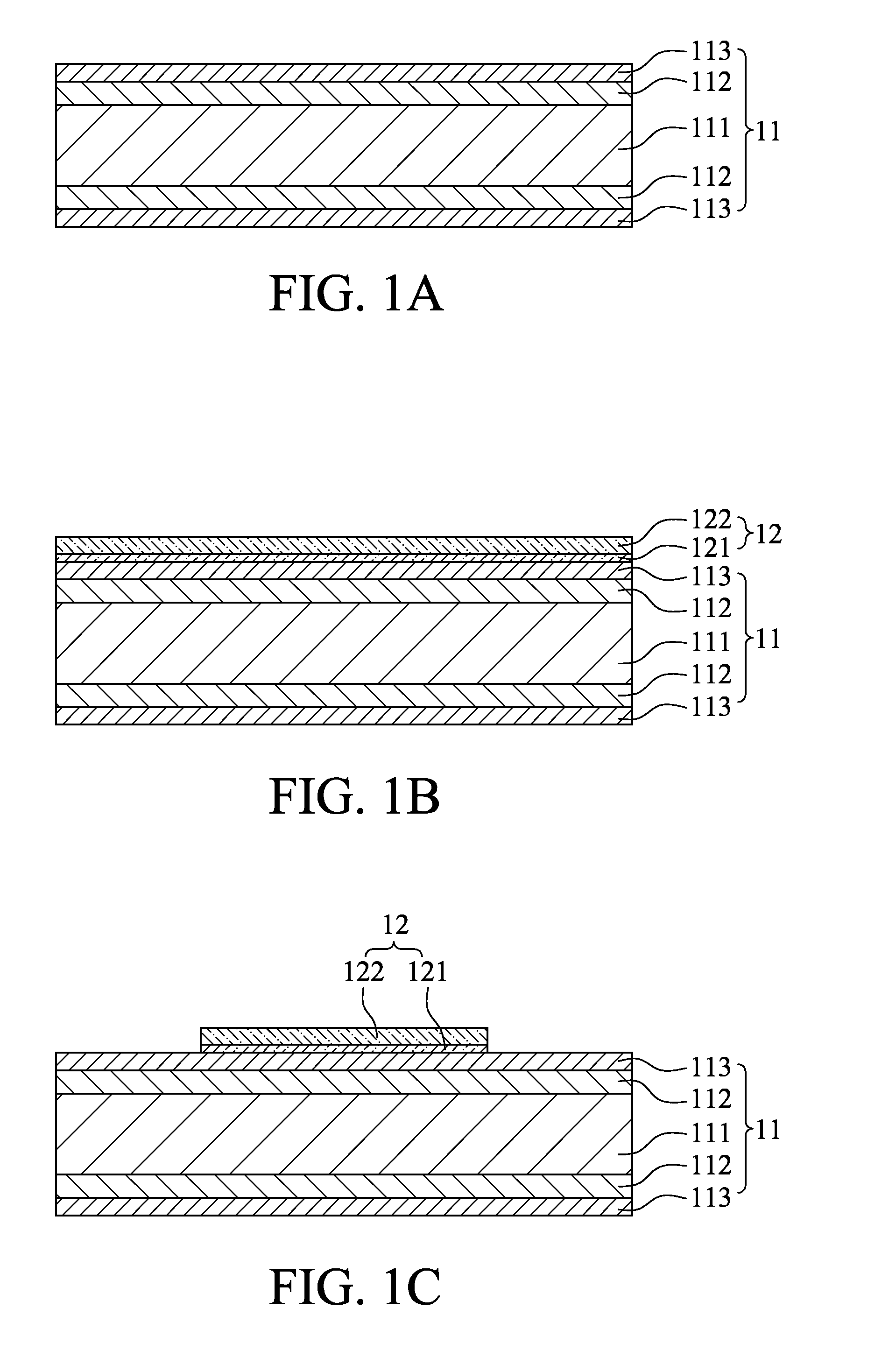
[0015]Referring from FIG. 1A to 1J, manufacturing method for a Zinc Oxide piezoelectric thin-film 10 with high C-axis orientation in accordance with an embodiment of this invention comprises the steps of: first, with reference to FIG. 1A, providing a substrate 11 having a base 111, a SiO2 layer 112 and a Si3N4 layer 113, in this embodiment, the substrate 11 can be a Si substrate; next, with reference to FIG. 1B, forming a bottom electrode layer 12 on the Si3N4 layer 113 of the substrate 11; with reference to FIG. 1C, patterning the bottom electrode layer 12; with reference to FIG. 1D, sputtering a Zinc Oxide layer 13 on the Si3N4 layer 113 of the substrate 11 and the bottom electrode layer 12, parameters for sputtering the Zinc Oxide layer 13 include substrate temperature, oxygen / argon ratio, sputtering power and base pressure, wherein the substrate temperature is within the range from 250 to 350 degrees C., the oxygen / argon ratio is within the range from 20% to 25%, the sputtering ...


PUM

PropertyMeasurementUnit
thicknessaaaaaaaaaa
thicknessaaaaaaaaaa
piezoelectricaaaaaaaaaa

Abstract

A manufacturing method for a Zinc Oxide (ZnO) piezoelectric thin-film with high C-axis orientation comprises the steps of providing a substrate having a base, a SiO2 layer and a Si3N4 layer; forming a bottom electrode layer on the Si3N4 layer; patterning the bottom electrode layer; sputtering a Zinc Oxide layer on the Si3N4 layer and the bottom electrode layer; forming a photoresist layer on the Si3N4 layer and the Zinc Oxide layer; patterning the photoresist layer to reveal the Zinc Oxide layer; forming a top electrode layer on the Zinc Oxide layer and the photoresist layer; removing the photoresist layer and the top electrode layer formed on the photoresist layer, and the top electrode layer formed on the Zinc Oxide layer can be remained; and patterning the Si3N4 layer to form a recess that reveals the base of the substrate.

Description

FIELD OF THE INVENTION[0001]The present invention is generally relating to a piezoelectric thin-film, more particularly to a Zinc Oxide piezoelectric thin-film with high C-axis orientation.BACKGROUND OF THE INVENTION[0002]A conventional piezoelectric thin-film is utilized to regard as sensing device by theory of acoustic resonance, wherein quartz crystal microbalance (QCM) has been utilized extensively in the field of piezoelectric sensor. Quartz crystal microbalance technology detects a mass by change in resonant frequency of a quartz crystal. The resonant frequency of the quartz crystal drops when a sampling object is absorbed on an electrode surface of the quartz crystal. By obtaining a resonant frequency offset from the quartz crystal and quantity of the molecules from the sampling object, the quantity of the molecules absorbed by the quartz crystal is able to require. The QCM technology has good linearity and is insensitive to temperature. However, QCM technology is not compati...

Claims


Application Information

Patent Timeline
Patent Type & Authority Patents(United States)
IPC IPC(8): H01L41/22H01L41/18H10N30/01H10N30/85
CPCC23C14/086H01L41/187H01L41/314H10N30/853H10N30/074Y10T29/42Y10T29/49155Y10T29/49156
Inventor HUANG, I-YULIN, CHANG-YUCHEN, YU-HUNG
Owner NAT SUN YAT SEN UNIV
Learn More