Driving method of semiconductor device
a driving method and semiconductor technology, applied in semiconductor devices, digital storage, instruments, etc., can solve the problems of reducing the reliability of storage devices, and achieve the effect of improving the reliability of semiconductor devices, stable writing, and stable holding
- Summary
- Abstract
- Description
- Claims
- Application Information
AI Technical Summary
Benefits of technology
Problems solved by technology
Method used
Image
Examples
embodiment 1
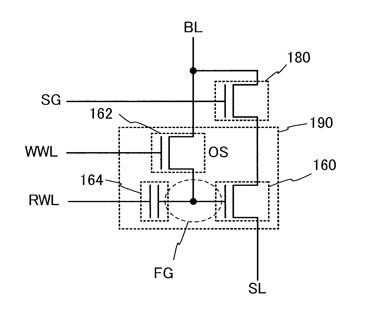
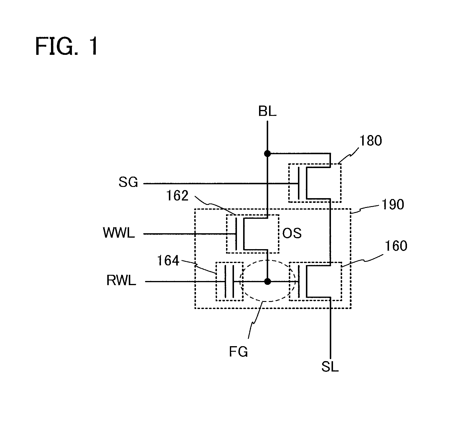
[0071]In this embodiment, a circuit configuration and operation of a semiconductor device according to one embodiment of the invention disclosed herein will be described with reference to FIG. 1. Note that in a circuit diagram, in some cases, “OS” is written beside a transistor in order to indicate that the transistor includes an oxide semiconductor material.
[0072]First, a basic circuit configuration and circuit operation will be described with reference to FIG. 1. In the circuit diagram in FIG. 1, one of a source electrode and a drain electrode (e.g., the drain electrode) of a selection transistor 180, one of a source electrode and a drain electrode (e.g., the drain electrode) of a transistor 162, and a bit line BL are electrically connected to one another. The other of the source electrode and the drain electrode (e.g., the source electrode) of the selection transistor 180 is electrically connected to one of a source electrode and a drain electrode (e.g., the drain electrode) of a...
application example
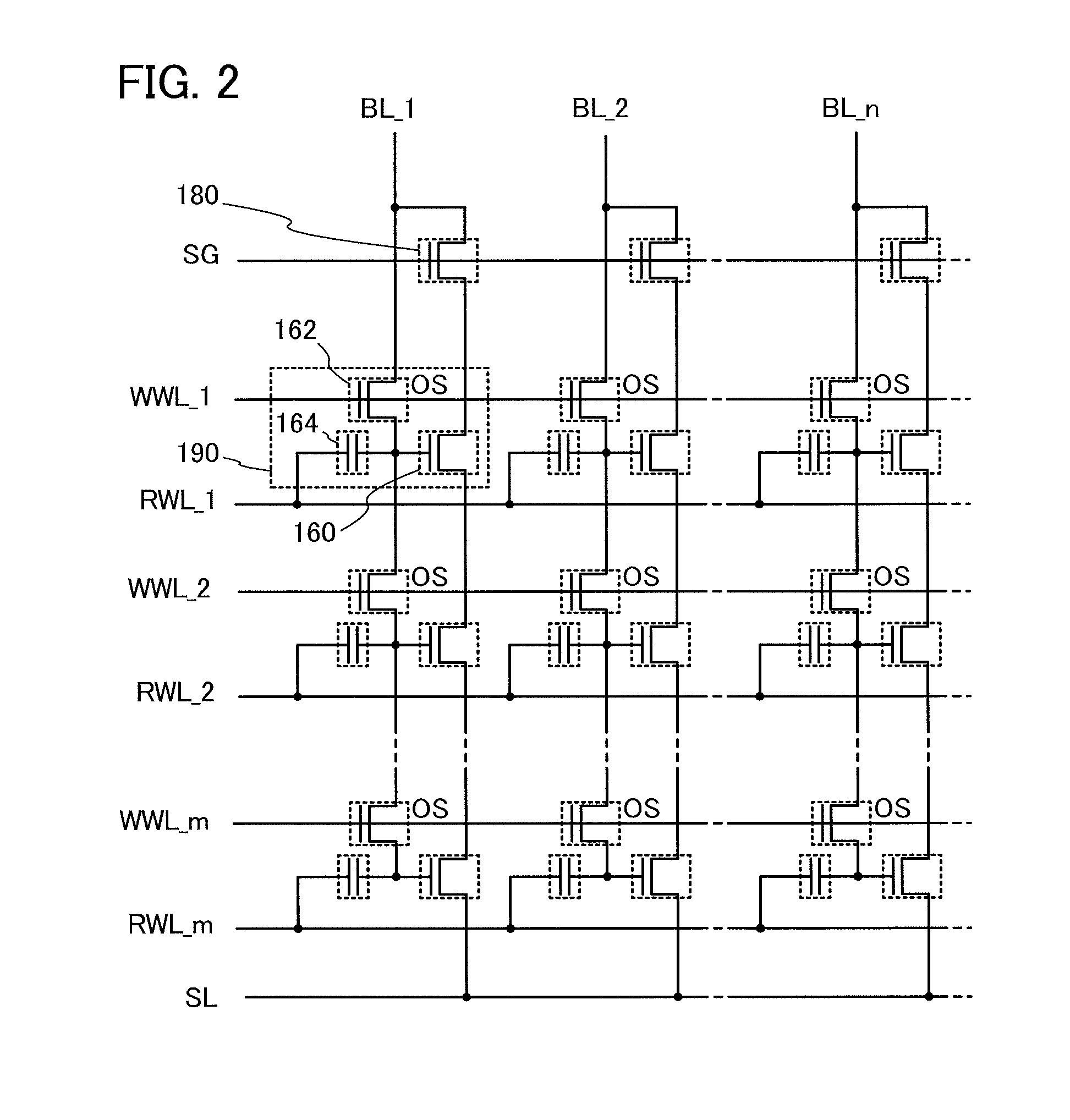
[0094]Next, a circuit configuration to which the circuit illustrated in FIG. 1 is applied and its operation will be described with reference to FIG. 2 and FIG. 3.
[0095]FIG. 2 illustrates an example of a circuit diagram of a NAND-type semiconductor device including m rows (in a vertical direction)×n columns (in a horizontal direction) memory cells 190 (m is a natural number greater than or equal to 2 and n is a natural number). Note that actually, the semiconductor device can include a plurality of sets of m (rows) (in a vertical direction)×n (columns) (in a horizontal direction) cells. In FIG. 2, wirings having a similar function are distinguished by “1”, “2”, and the like added to the end of their names.
[0096]The semiconductor device in FIG. 2 includes m writing word lines WWL (WWL1 to WWLm), m reading word lines RWL (RWL1 to RWLm), n bit lines BL (BL1 to BLn), a memory cell array in which the m rows (in a vertical direction)×n columns (in a horizontal direction) memory cells 190 a...
embodiment 2
[0144]In this embodiment, a circuit configuration and operation of a semiconductor device according to one embodiment of the invention disclosed herein will be described with reference to FIG. 4. Note that in a circuit diagram, “OS” is written beside a transistor in order to indicate that the transistor includes an oxide semiconductor material.
[0145]The circuit configuration shown in FIG. 4 is an example of a circuit configuration of a NAND-type semiconductor device including r (in a vertical direction)×n (in a horizontal direction) blocks 700 (r is a natural number greater than or equal to 1), in which one block includes in memory cells 190 and a selection transistor 180. The configuration of the block 700 in FIG. 4 is similar to the configuration in FIG. 2. Note that either the source electrodes or drain electrodes of the selection transistors 180 in each of the r blocks 700 electrically connected in the vertical direction are electrically connected to the same bit line BL.
[0146]I...
PUM
 Abstract
Description
Claims
Application Information
 - R&D
- Intellectual Property
- Life Sciences
- Materials
- Tech Scout
- Unparalleled Data Quality
- Higher Quality Content
- 60% Fewer Hallucinations
Browse by: Latest US Patents, China's latest patents, Technical Efficacy Thesaurus, Application Domain, Technology Topic, Popular Technical Reports.
© 2025 PatSnap. All rights reserved.Legal|Privacy policy|Modern Slavery Act Transparency Statement|Sitemap|About US| Contact US: help@patsnap.com


