Bulk low-cost interface-defined laminated materials and their method of fabrication

a laminated material and low-cost technology, applied in the field of low-cost interface-defined laminated materials and their method of fabrication, can solve the problems of inability to forge, many metals are too hard and brittle, etc., and achieve the effects of preventing the system from coarsening, increasing the feature size, and unique gains in high-temperature oxidation and reaction stability

Inactive Publication Date: 2013-12-31
THE UNITED STATES OF AMERICA AS REPRESETNED BY THE SEC OF THE AIR FORCE
View PDF86 Cites 2 Cited by
  • Summary
  • Abstract
  • Description
  • Claims
  • Application Information

AI Technical Summary

Benefits of technology

[0025]Moreover, it should be noted that, if properly designed from the thermodynamic point of view, so that only phases with no- or limited-solid state solubility are present, the Interface-Defined Nano-Laminates of the instant invention can have a lot in common thermodynamically with spinodal structures found in nature. That is, these spinodal structures can have similar nanostructural interfacial features, and also are known to have remarkable phase stability at high temperature. From this discussion, it should be clear that not all attractive material combinations could be used as adjacent layers because of the thermodynamic stability requirement. The exact combination of the materials has to be deduced from corresponding phase diagrams to assure that the phases are stable at the temperatures required for processing and service. In fact, these artificially made nanostructures, if properly designed thermodynamically, should inherit a lot of stability features of spinodal structures, including thermal, chemical, and mechanical stability. It is known that spinodal structures greatly resist any kind of thermo-chemical changes because they are, at any given temperature, at kinetically-stable state. From the mechanical point of view, spinodals are usually highly resistant to crack nucleation and growth because, as all layered structures, they are susceptible to crack branching and crack-tip blunting. Accordingly, the Interface-Defined Nano-Laminates that are the subject of this invention are also expected to have significantly increased fracture toughness as represented in increased resistance to crack nucleation and crack propagation. All this should lead to greatly improved mechanical strength, flaw tolerance, and thermal shock resistance.
[0028]The enthalpy change term in (2), dH, is always negative with coarsening, thus driving the system towards increasing its feature size. However, the change of enthropy term, −TdS, is positive on coarsening, and can be made sufficiently large, to override the dH term and make dG>0, thus preventing the system from coarsening. This can be achieved by the judicious selection of the components of the nanolayered material, thus decreasing the Gibbs free energy of the nanolayered material to the point that any increase in feature size is thermodynamically unfavorable, and giving increased thermal stability to the nanosize material.
[0029]It is quite scientifically unexpected and fortuitous that the force driving the system towards equilibrium can be increased as the dimensions decrease by the careful selection of the components, which maximizes the entropy of the interface. That is, by utilizing the nanoscale layers, the number of interfaces, and, especially, the type of the interface between the dissimilar layers in the material, the disorder in the material is greatly increased, which in turn increases the entropy of the system. Subsequently, the thermal stability is increased because of decreasing Gibbs free energy (delta H-T delta S in equation (2). The novelty, uniqueness, and power of this approach, which we term “Entropic Stabilization” lies in activating the true capabilities of the nanoscopic structuring made possible by using the appropriate thermodynamic considerations that arise only in dissimilar nanostructured materials, and utilizing the unique processing approach outlined below to achieve such nanostructures in the bulk.
[0030]There are many unique aspects of the instant invention. One aspect of the uniqueness of the approach is in its capability of manufacturing large, bulk, quantities of materials at relatively low cost that currently are fabricated in small quantities by very expensive techniques. Another aspect of the uniqueness of this approach is in its ability to design, control, and optimize composition and properties of the interfaces, rather than the bulk of the nanophase grains.
[0031]Thus, the use of methods described in this invention, offers unprecedented opportunities in fabricating bulk quantities of materials that currently exist only as small research samples, because of the prohibitively expensive fabrication techniques.

Problems solved by technology

Unfortunately, most ceramic materials and many metals are much too hard and brittle, even at very high temperatures (500-1200° C.) to allow such processing.
In other words—they do not deform plastically, making forging impossible.

Method used


Image

  • Bulk low-cost interface-defined laminated materials and their method of fabrication
  • Bulk low-cost interface-defined laminated materials and their method of fabrication
  • Bulk low-cost interface-defined laminated materials and their method of fabrication

Examples


example 1

Modeling

[0041]The first step in the process of fabricating an IDnL material is to make the decision on the type of interface properties this material should have. For example, if the projected material is a thermal insulator intended for exploitation at very high temperatures, the properties of the interfaces must include thermodynamic stability, or at least kinetic stability for specified duration at service temperatures. All mechanisms of heat transport must be taken into consideration: in this case phononic and photonic, and the reflection and transmission coefficients at the designed interfaces evaluated. Also, some estimates of the degree of coherency should be performed. After this 1st step, the composition of the materials in the layers, the exact sequence of the dissimilar layers, the structure and chemistry of the interfaces, the thickness of each type of the alternating layers in the direction perpendicular to the plane of the layers, the density of layers per unit of thic...

example 2

Solid Electrolytes with Improved Ionic Conductivity

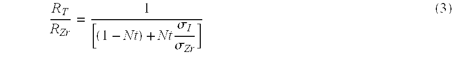
[0066]The use of IDnL materials is a very promising approach to generate a whole new family of Fast Ion Conducting materials that can be used as solid electrolytes in gas electrolyzers, electrochemical pumps, gas sensors, catalytic reactors, and most importantly in fuel cells. Production of energy from fuel cells utilizing ethanol, methanol, natural gas, coal products, etc. is of great national importance for use in transportation, stand-alone power, and residential power to name a few. Although this technology has broad application, such as in cation-conductors (lithium and sodium solid electrolytes), we will take as an example, oxygen ion conduction, for which the most commonly utilized solid electrolyte is yttria stabilized zirconia (YSZ). Although YSZ is the workhorse of the Oxygen Fuel Cell industry, the low oxygen conductivity at temperatures below 800° C. is the major problem causing huge inefficiencies due to the thermal los...

example 3

Novel Semiconductor Materials

[0097]Novel semiconducting materials that will play a major role in several new technologies such as nonlinear optics, luminescence, electronics, catalysis, solar energy conversion, and optoelectronics are amendable to manufacturing using the instant invention. It is well-known that the small dimensions of nanosize particles of semiconductors, such as CdS and CdSe, for example, result in different physical properties from those observed in the “bulk” material. However, manufacturing bulk pieces from these materials is complicated. Our approach, however, is naturally amenable to manufacturing large samples. In this example, the semiconducting material forms one laminate layer while thiophenol or another material, which allows for pressure-assisted consolidation and nano-assembly, forms the adjacent nano-laminate layer. The interfaces between the two different laminates layers can be designed to generate specific energy levels for electrons or holes, or ev...


PUM

PropertyMeasurementUnit
thicknessaaaaaaaaaa
porosityaaaaaaaaaa
thicknessaaaaaaaaaa

Abstract

This invention describes a novel type of materials named by the inventors as Interface-Defined nano-Laminates (IDnL), and a new method for fabricating these materials from ceramic, metallic, and other powders. The laminate layer thickness in IDnL is smaller than that of ordinary laminates, but greater than that of superlattices. IDnL are fundamentally different from ordinary laminates in that their properties are defined by interfaces, and not by the properties of the bulk materials comprising individual layers. In contrast to superlattice materials, IDnL can be made thermally stable, due to the wide selection of interface-defining materials, which allows judicial use of equilibrium phase diagrams, and the “entropic stabilization” approach discovered by the authors; and in addition IDnL can be manufactured inexpensively in bulk, industrial quantities and large sizes by the techniques revealed in this invention. The degree of interface coherency in an IDnLs can be varied to optimize material properties.

Description

CROSS REFERENCE TO RELATED APPLICATION[0001]This application is a continuation-in-part of and claims priority from U.S. patent application Ser. No. 12 / 728,293 filed on Mar. 22, 2010.RIGHTS OF THE GOVERNMENT[0002]The invention described herein may be manufactured and used by or for the Government of the United States for all governmental purposes without the payment of any royalty.BACKGROUND OF INVENTION[0003]The present invention describes a novel class of materials that fits between the ordinary industrial laminates and research-type nanolaminates or superlattices, in regards to properties and cost. The novel Interface-Defined nano-Laminated materials (IDnL) of this invention differ from both the large-scale laminates and the extremely fine-scale superlattices, due to their unique micro- and nano-structures produced by the novel methods of fabrication, which are also a subject of this invention. In the new IDnL materials, the interfaces between the alternative layers can be designe...

Claims


Application Information

Patent Timeline
Patent Type & Authority Patents(United States)
IPC IPC(8): B28B1/30
CPCB28B1/16C04B2235/77C04B2237/348B32B18/00B32B19/048C04B2237/704C04B2237/36C04B35/645B82Y40/00C04B2237/58C04B2235/768C04B2237/346C04B2235/762
Inventor PECHENIK, ALEXANDERHOFFMAN, WESLEY P.
Owner THE UNITED STATES OF AMERICA AS REPRESETNED BY THE SEC OF THE AIR FORCE
Why Eureka
Try Eureka