Wiring structure, display apparatus, and semiconductor device
a display device and wiring technology, applied in the direction of semiconductor devices, semiconductor/solid-state device details, electrical apparatus, etc., can solve the problems of increased production cost, reduced productivity, signal delay and power loss attributable to high wiring resistance, etc., to achieve excellent contact resistance, increase process margins, and high productivity
- Summary
- Abstract
- Description
- Claims
- Application Information
AI Technical Summary
Benefits of technology
Problems solved by technology
Method used
Image
Examples
first embodiment
of the Present Invention
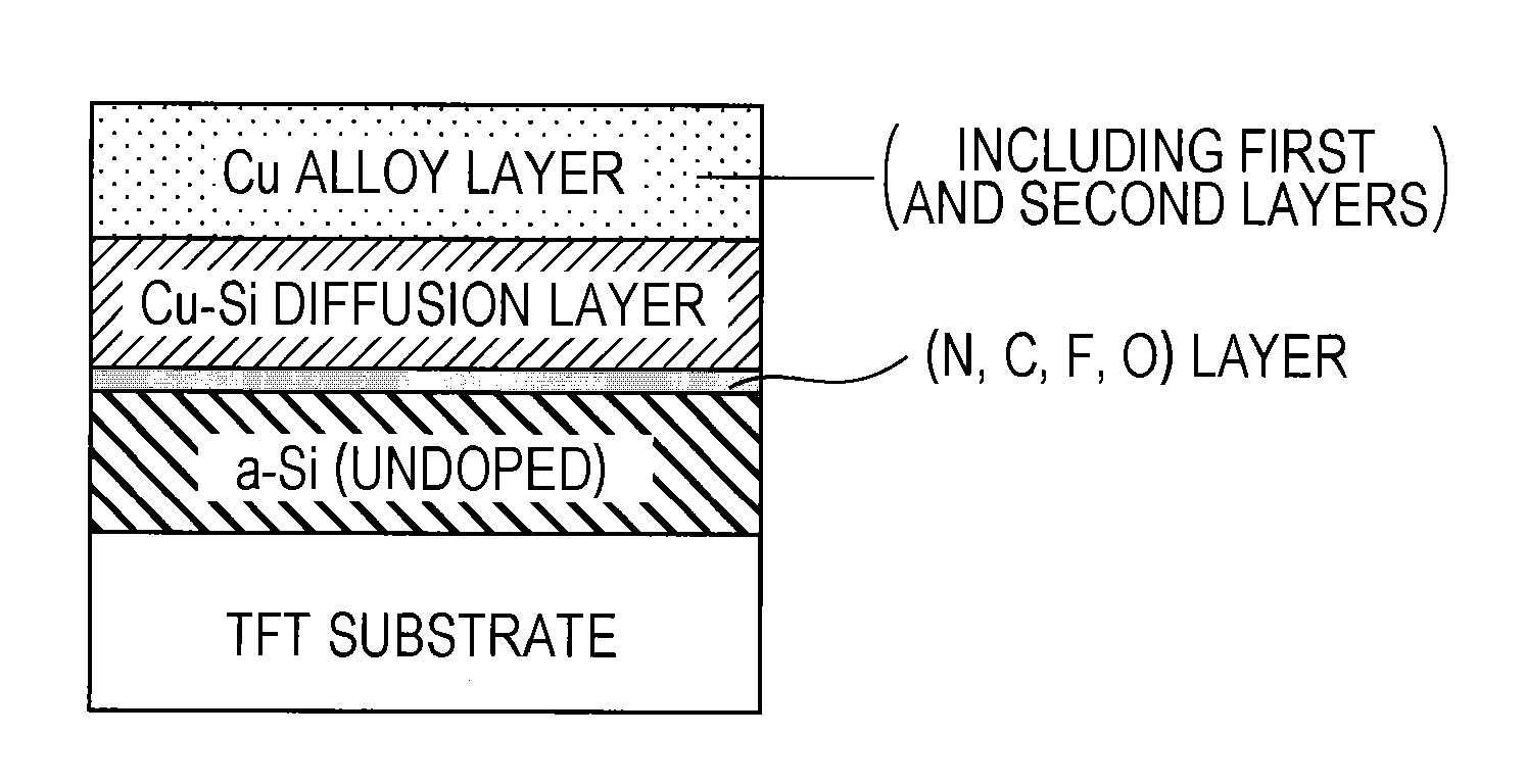
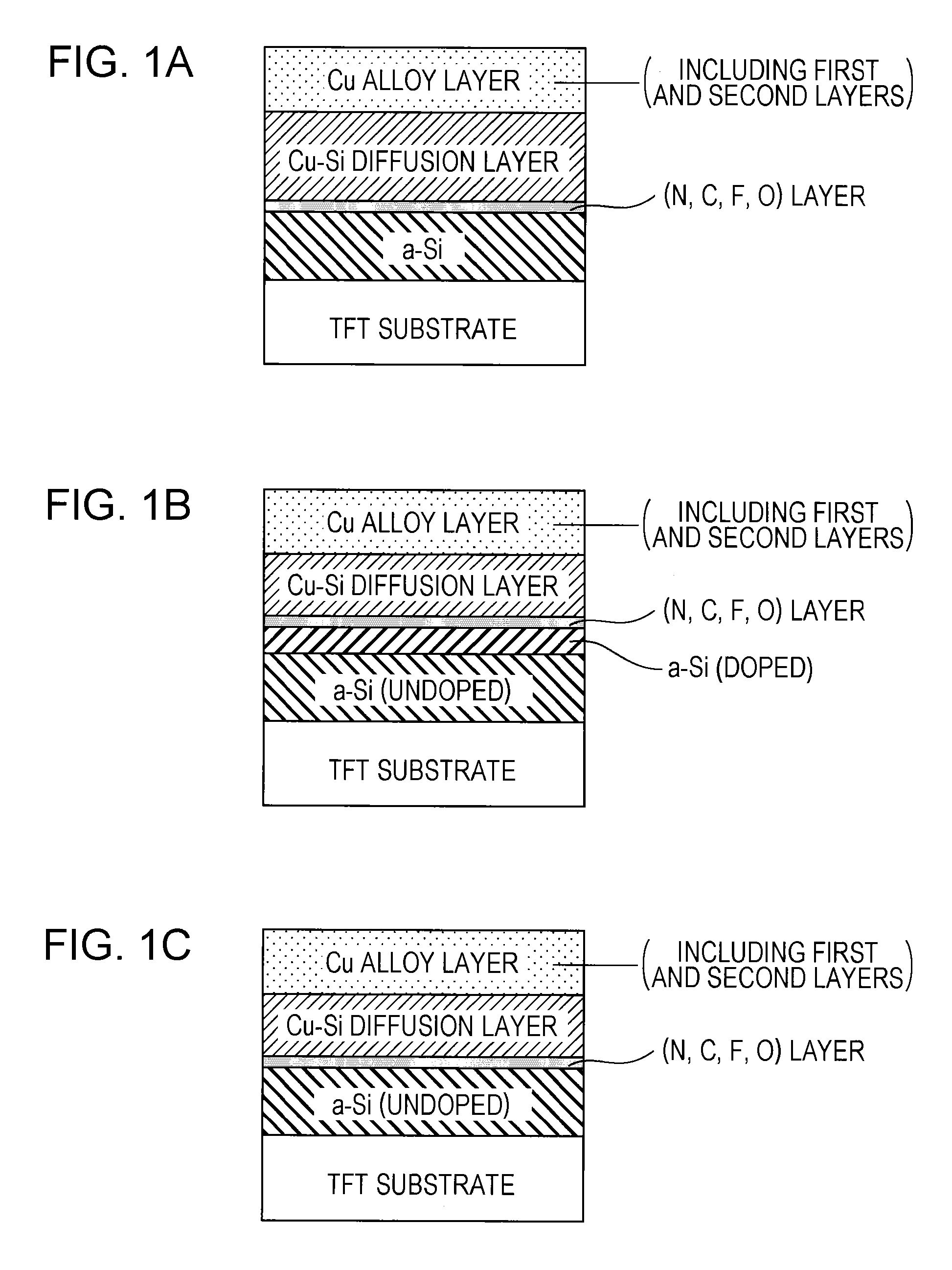
[0045]A first embodiment of the TFT according to the present invention is shown in FIG. 1A. A structure shown in FIG. 1A includes a first semiconductor layer on a TFT substrate; a two-layer structure directly on the first semiconductor layer, the two-layer structure including a (N, C, F, O) layer and a Cu—Si diffusion layer; and a Cu alloy layer (including a first layer and a second layer) directly on the two-layer structure. The structure shown in FIG. 1A is obtained by forming a (N, C, F, O) layer, then forming a second semiconductor layer and a Cu alloy layer (multilayer structure), and then applying a heat history at about 150° C. or higher.
[0046]In the first embodiment, the (N, C, F, O) layer contains at least one element selected from the group consisting of nitrogen, carbon, fluorine, and oxygen. Since the (N, C, F, O) layer is formed so as to substantially cover the entire surface of the semiconductor layer, the (N, C, F, O) layer effectively serves a...
second embodiment
of the Present Invention
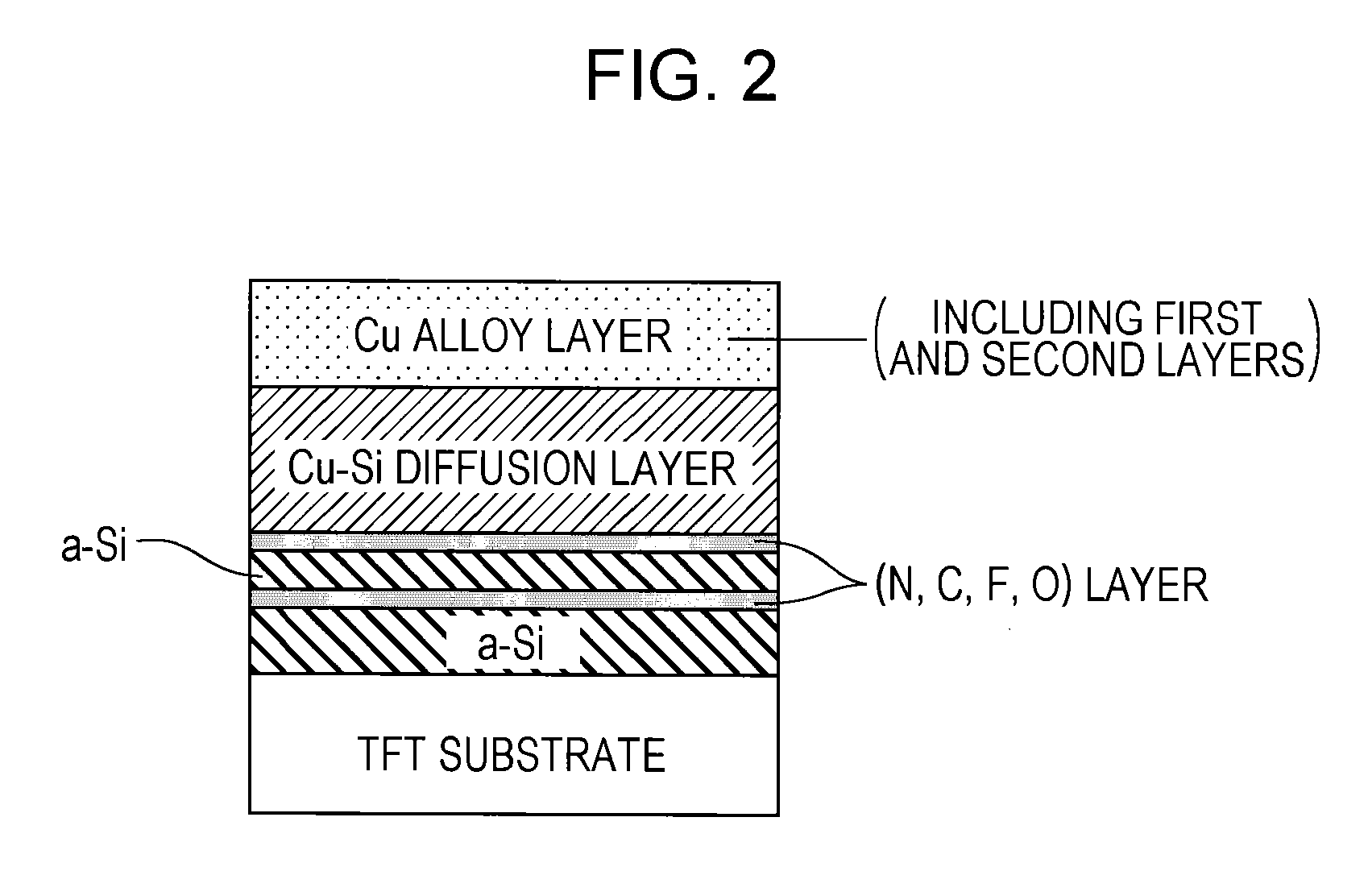
[0083]A second embodiment of the TFT according to the present invention is an example that has a first semiconductor layer, a (N, C, F, O) layer, and another first semiconductor layer between the TFT substrate and the (N, C, F, O) layer constituting the two-layer structure in the first embodiment described above. In particular, as shown in FIG. 2, a first semiconductor layer, a (N, C, F, O) layer, and another first semiconductor layer are stacked in that order on a TFT substrate, a two-layer structure including a (N, C, F, O) layer and a Cu—Si diffusion layer is disposed thereon, and a Cu alloy layer is directly formed on the two-layer structure.
third embodiment
of the Present Invention
[0084]A first embodiment of a MOSFET according to the present invention is shown in FIG. 4. In FIG. 4, a two-layer structure including a (N, C, F, O) layer and a Cu—Si diffusion layer is directly formed on single crystal Si and a Cu alloy layer is directly formed on the two-layer structure. This structure is formed by the steps shown in FIG. 5. That is, among N, C, F, and O, for example, nitrogen is implanted into a single crystal Si substrate by an ion implantation method or the like. During this process, implanted nitrogen exhibits a substantially Gaussian distribution in the depth direction around a particular depth (referred to as trajectory). Part of Si becomes amorphous by damage done by implanted nitrogen. Next, a Cu alloy layer is formed by sputtering and plating and then a heat treatment such as annealing is performed to form a Cu alloy layer (including first and second layers) / Cu—Si diffusion layer / nitrogen-containing layer / single crystal Si structu...
PUM
| Property | Measurement | Unit |
|---|---|---|
| thickness | aaaaa | aaaaa |
| distance | aaaaa | aaaaa |
| distance | aaaaa | aaaaa |
Abstract
Description
Claims
Application Information
 - R&D
- Intellectual Property
- Life Sciences
- Materials
- Tech Scout
- Unparalleled Data Quality
- Higher Quality Content
- 60% Fewer Hallucinations
Browse by: Latest US Patents, China's latest patents, Technical Efficacy Thesaurus, Application Domain, Technology Topic, Popular Technical Reports.
© 2025 PatSnap. All rights reserved.Legal|Privacy policy|Modern Slavery Act Transparency Statement|Sitemap|About US| Contact US: help@patsnap.com


