
Organic EL device and method for manufacturing same

a technology of organic el and display apparatus, which is applied in the direction of organic semiconductor devices, solid-state devices, thermoelectric devices, etc., can solve the problems of difficult mass-production of large organic el displays of 100-inch class, difficult to accurately maintain the arrangement of masks for each color, and inferior light emitting layer formed by vapor deposition to crystal liquid displays. achieve the effect of retaining the lyophobicity of the bank

Active Publication Date: 2013-09-10
JOLED INC
View PDF26 Cites 5 Cited by
  • Summary
  • Abstract
  • Description
  • Claims
  • Application Information

AI Technical Summary

Benefits of technology

This approach effectively removes bank residues from the hole injection layer while preserving the lyophobicity of the bank, enabling the production of high-productivity organic EL devices with improved device characteristics and scalability to larger panels like the 100-inch class.

Problems solved by technology

However, it is difficult to mass-produce a large organic EL display of 100-inch class by the manufacturing technique of the organic EL device using this vacuum process.
This is because it is difficult to accurately maintain the arrangement of a mask for each of the colors used for forming the light emitting layer by vapor deposition (for example, red (R), green (G), and blue (B)).
Further, the organic EL display having the light emitting layer formed by vapor deposition is inferior to a crystal liquid display, which competes with the organic EL display, in cost, and thus further improvement has been desired.
Accordingly, unlike the case in which the light emitting layer is formed by vacuum deposition, a problem of non-uniformity of coating or a problem arisen by distortion of metal masks used for patterning a deposition layer will not occur.
Further, as the substrate becomes larger, it will be difficult to perform plasma treatment uniformly on the substrate in the direction of the plane of the substrate, causing variation of lyophobicity of the bank in the direction of plane of the substrate.

Method used


Image

  • Organic EL device and method for manufacturing same
  • Organic EL device and method for manufacturing same
  • Organic EL device and method for manufacturing same

Examples


experimental example 1

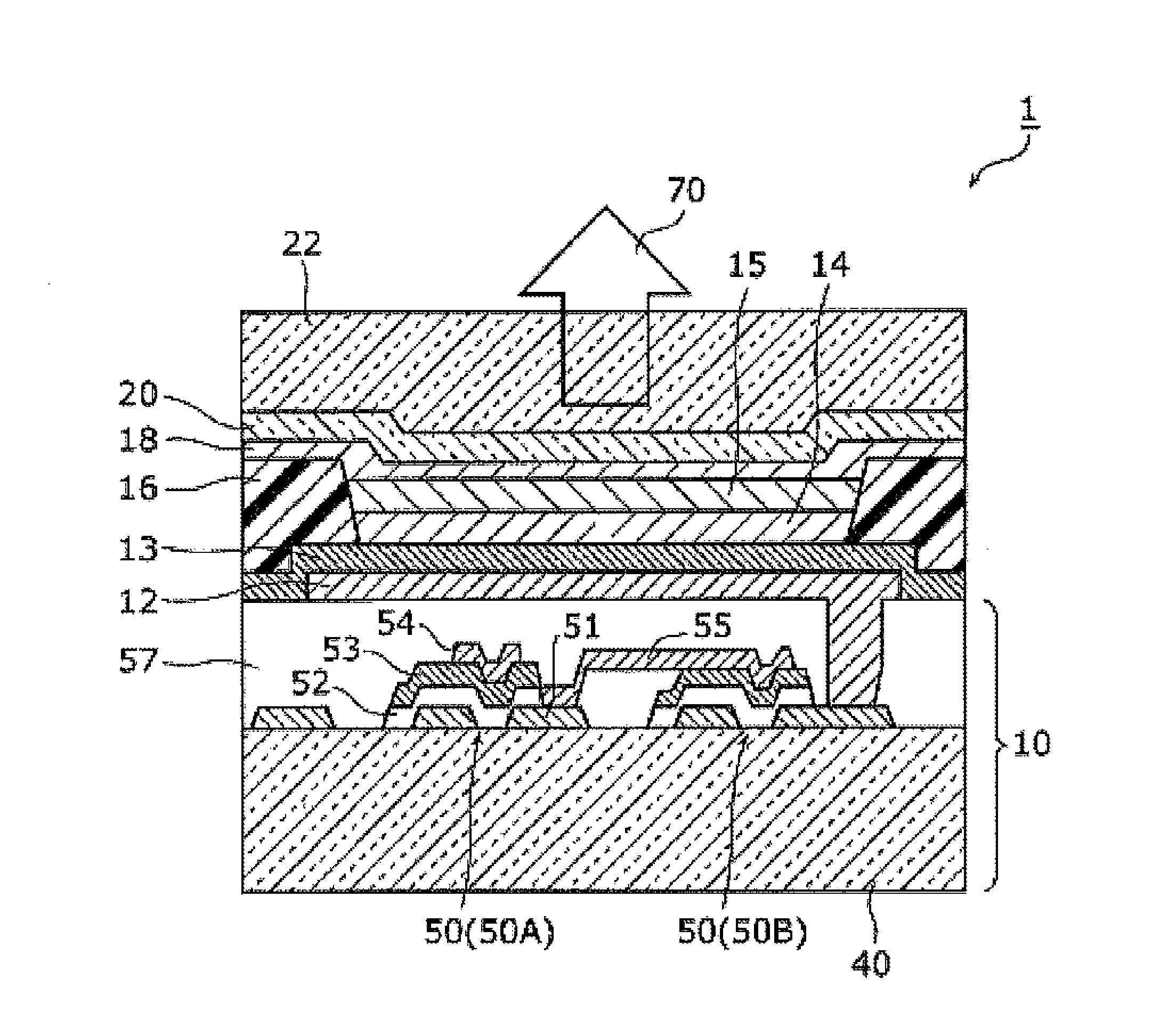
[0169]Titanium oxide (TiOx) film having a thickness of 50 nm is formed by sputtering on a glass substrate measuring 100 mm per side (EAGLE 2000, Matsunami Glass Ind., Ltd.) as a model of the hole injection layer. The deposition condition is set as follows: the target is sintered TiO2, the Ar gas pressure is around 1 Pa, and RF output is 300 W.

[0170]A bank is formed on the formed titanium oxide (TiOx) film by photolithography. An acrylic resin (Asahi Glass Co., Ltd.), the acrylic resin containing fluorine compounds, is used as a material of the bank. Further, as the material of the bank, a negative material, which undergoes cross-link reaction and is cured when being exposed with a light, is used. The bank is patterned a film formed by spin coating by pre-baking a film formed by spin coating at the temperature of 100° C. for two minutes; irradiating the film with ultraviolet light via a photomask; and developing the film using 0.2% of a Tetra Methyl Ammonium Hydroxide (TMAH) aqueous ...


PUM


Abstract

Disclosed is an organic EL device which comprises: a pixel electrode that is arranged on a substrate; a hole injection layer that is arranged on the pixel electrode and has a photocatalytic function; an organic functional layer that is formed on the hole injection layer by a coating method; a bank made of a fluorine-containing resin and defines the region where the organic functional layer is arranged; and a counter electrode that is arranged so as to cover the bank and the organic functional layer. Due to the photocatalytic function of the hole injection layer, the bank residuals can be removed by low-energy ultraviolet light that has a longer wavelength (300-400 nm) than conventional high-energy ultraviolet light that has a short wavelength (254 nm or 172 nm).

Description

TECHNICAL FIELD[0001]The present invention relates to an organic EL device and display apparatus including the organic EL device and relates to methods of manufacturing the same.TECHNICAL FIELD[0002]Various electronic devices such as a luminescent device, a solar cell, other semiconductor devices have been actively studied and developed. Among the electronic devices, the organic EL device, one of the organic electronic devices having an organic functional layer is expected to be applied to a next-generation thin display, and in recent years the organic EL device has been extremely actively studied.[0003]The organic EL device has a structure in which an organic functional layer having a light emitting layer is placed between an anode and a cathode. In the organic EL device, holes and electrons are injected from the anode and the cathode, respectively, into the light emitting layer and the holes and the electrons are recombined in the light emitting layer to emit a light. The organic ...

Claims


Application Information

Patent Timeline
Patent Type & Authority Patents(United States)
IPC IPC(8): H01L33/00
CPCH01L51/5088H01L27/3246H01L2227/323H01L2251/5315H01L2251/568H10K59/122H10K50/17H10K2102/3026H10K59/1201H10K71/861H10K59/121
Inventor NAKATANI, SHUHEIHIGASHIDA, TAKAAKI
Owner JOLED INC
Learn More