Semiconductor element, semiconductor device, and method for manufacturing the same
a semiconductor and semiconductor technology, applied in the direction of semiconductor devices, electrical devices, transistors, etc., can solve the problems of difficult manufacturing a minute semiconductor element, limited space between the source electrode layer and the drain electrode layer through a photo process, etc., to achieve the effect of reducing power consumption, improving circuit operation speed, and improving coverage with a gate insulating layer
- Summary
- Abstract
- Description
- Claims
- Application Information
AI Technical Summary
Benefits of technology
Problems solved by technology
Method used
Image
Examples
embodiment 1
[0072]In this embodiment, an example of a cross-sectional structure of a semiconductor element according to one embodiment of the present invention will be described.
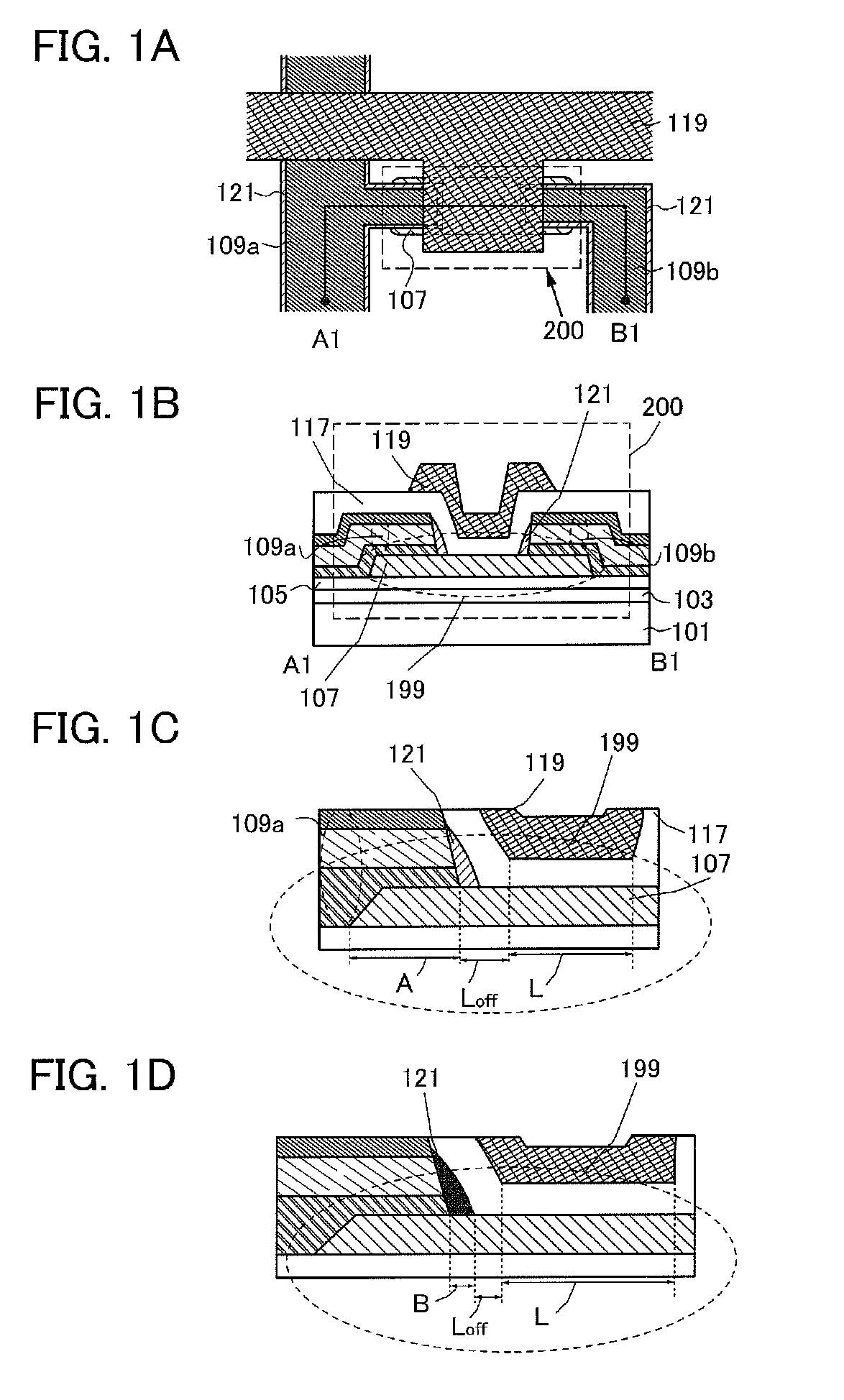
[0073]A semiconductor element of this embodiment will be described with reference to FIGS. 1A to 1D and FIGS. 28A and 28B. FIG. 1A is a top view of a semiconductor element of one embodiment of the present invention. FIG. 1B is a cross-sectional view taken along a line A1-B1 in FIG. 1A. FIGS. 1C and 1D are enlarged views of a dashed line portion 199 in FIG. 1B. In addition, FIGS. 28A and 28B each illustrate an example of a cross-sectional structure of a semiconductor element of one embodiment of the present invention. A transistor 200 illustrated in FIGS. 1A to 1D, a transistor 201 illustrated in FIG. 28A, and a transistor 300 illustrated in FIG. 28B are top-gate transistors.
[0074]The transistor 200 illustrated in FIGS. 1A and 1B includes a first insulating layer 103, a second insulating layer 105, an oxide semiconductor...
embodiment 2
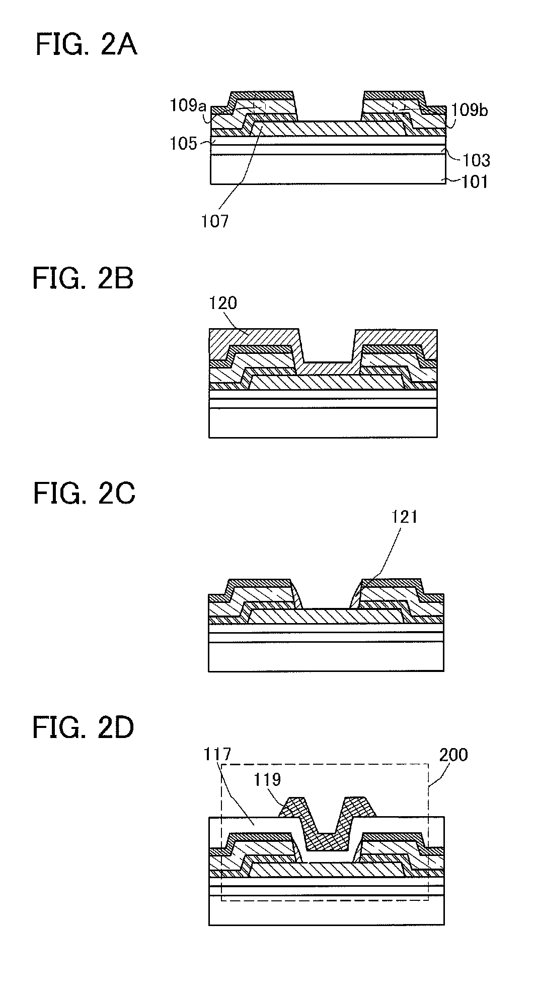
[0151]In this embodiment, an example of a method for manufacturing a semiconductor element will be described. One embodiment of a method for manufacturing a semiconductor element of this embodiment will be described with reference to FIGS. 2A to 2D.
[0152]A process of manufacturing the transistors 200 and 201, which are described in Embodiment 1, over the substrate 101 having an insulating surface will be described below.
[0153]Although there is no particular limitation on a substrate which can be used as the substrate 101 having an insulating surface, the substrate needs to have heat resistance high enough to withstand at least heat treatment performed later. For example, a glass substrate made of aluminosilicate glass, barium borosilicate glass, aluminoborosilicate glass, or the like can be used.
[0154]Note that a substrate formed of an insulator such as a ceramic substrate, a quartz substrate, or a sapphire substrate may be used instead of the glass substrate. Alternatively, a cryst...
embodiment 3
[0225]In this embodiment, a method for manufacturing a transistor which is different from that described in the above embodiment will be described with reference to drawings. Note that the manufacturing process (a material and the like which can be used) described in this embodiment has a lot in common with that described in Embodiment 2. Therefore, in the following description, description of the same portions will not be given, and different points will be described in detail.
[0226]The transistor 300 illustrated in FIG. 28B includes the first insulating layer 303, the second insulating layer 305, the oxide semiconductor layer 307, the first source electrode layer 309a, the second source electrode layer 311a, the first drain electrode layer 309b, the second drain electrode layer 311b, the third insulating layer 315, the sidewalls 321, the gate insulating layer 317, and the gate electrode layer 319 over the substrate 301 having an insulating surface.
[0227]An example of a method for ...
PUM
 Abstract
Description
Claims
Application Information
 - R&D
- Intellectual Property
- Life Sciences
- Materials
- Tech Scout
- Unparalleled Data Quality
- Higher Quality Content
- 60% Fewer Hallucinations
Browse by: Latest US Patents, China's latest patents, Technical Efficacy Thesaurus, Application Domain, Technology Topic, Popular Technical Reports.
© 2025 PatSnap. All rights reserved.Legal|Privacy policy|Modern Slavery Act Transparency Statement|Sitemap|About US| Contact US: help@patsnap.com


