
Method of forming nanoscale three-dimensional patterns in a porous material

a three-dimensional pattern and porous material technology, applied in the field of semiconductor fabrication, can solve the problems of large-area fabrication methods for producing nano-scale (100 nm) patterned porous silicon, inability to achieve spatial resolution of these techniques, and inability to achieve large-scale etching damage, etc., to achieve the effect of facilitating wafer level packaging integration

Active Publication Date: 2013-07-16
THE BOARD OF TRUSTEES OF THE UNIV OF ILLINOIS
View PDF18 Cites 36 Cited by
  • Summary
  • Abstract
  • Description
  • Claims
  • Application Information

AI Technical Summary

Benefits of technology

The patent describes a new way to create patterns on the surface of a porous material. This method has advantages over existing technologies and can be used to create devices with copper interconnects. It also helps with the packaging of these devices.

Problems solved by technology

The spatial resolution of these techniques may be limited by lithography tools or by the fragility and reactivity of porous silicon during formation or etching.
As a result, a large-area fabrication method for producing nanoscale (<100 nm) patterned porous silicon is still lacking.
However, the mechanical stability of the porous low-k material makes it susceptible to damage from etching and CMP.

Method used


Image

  • Method of forming nanoscale three-dimensional patterns in a porous material
  • Method of forming nanoscale three-dimensional patterns in a porous material
  • Method of forming nanoscale three-dimensional patterns in a porous material

Examples


example

[0046]Various nanoscale patterns, including dot, mesh, lines, grids, boomerang contour arrays in the range of from about 10 nm to about 100 nm in dimension, were written on PMMA on p− type (100) Si substrates (7 Ωcm) using electron beam lithography at 50 kV. Platinum (Pt) and titanium (Ti) metals were evaporated and followed with standard lift-off. Metal patterned substrates were then etched in a H2O2 metal-HF (HOME-HF) etchant for 15˜60 seconds. Morphology resulted from etching was examined with scanning electron microscopy (SEM) and atomic force microscopy (AFM). Optical properties of the etched samples were also characterized, as described in Chun et al., Applied Physics Letters 92, 191113 (2008) 1-3, which is hereby incorporated by reference in its entirety.

[0047]Shown in FIG. 3A is a SEM image of an array of Ti / Pt dots of 15 nm in height (5 nm Ti followed by 10 nm Pt), 15 nm in diameter and 100 nm in pitch patterned on a p− type silicon substrate. FIG. 3B shows the pattern afte...


PUM

PropertyMeasurementUnit
sizeaaaaaaaaaa
dielectric constantaaaaaaaaaa
angleaaaaaaaaaa

Abstract

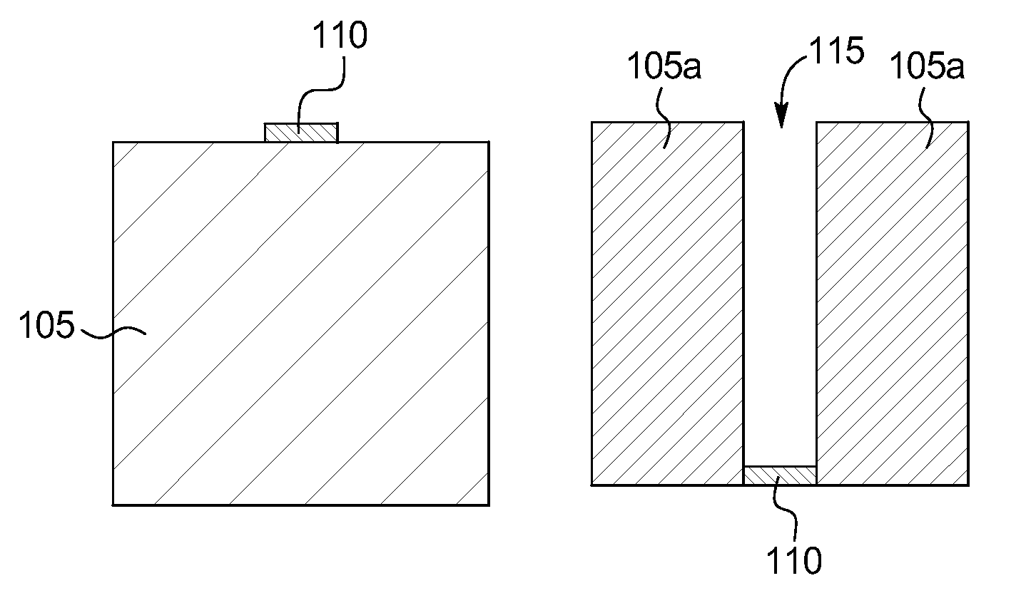
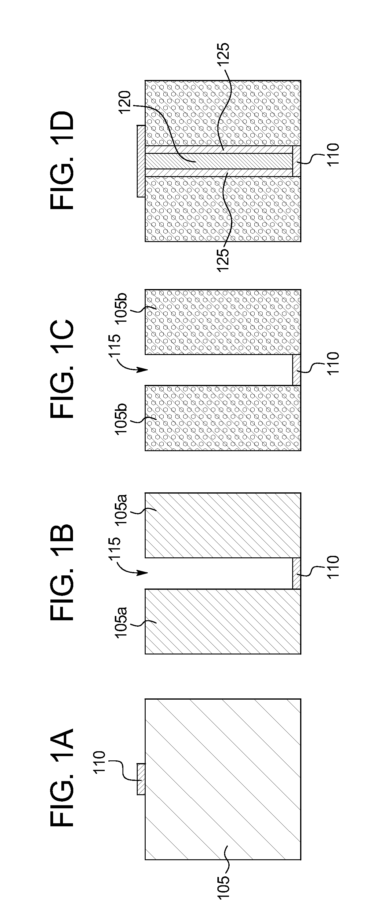
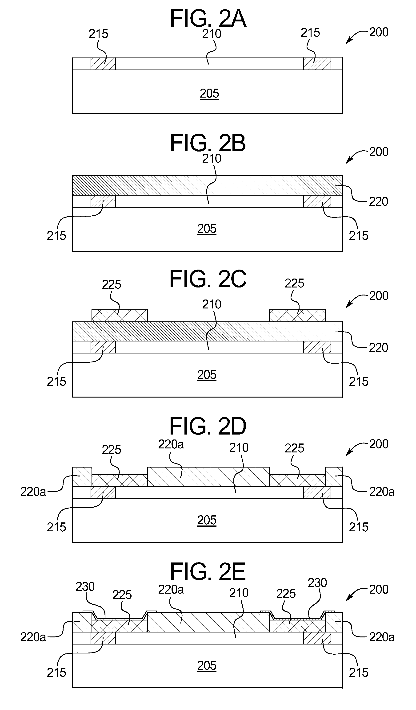
A method of forming a nanoscale three-dimensional pattern in a porous semiconductor includes providing a film comprising a semiconductor material and defining a nanoscale metal pattern on the film, where the metal pattern has at least one lateral dimension of about 100 nm or less in size. Semiconductor material is removed from below the nanoscale metal pattern to create trenches in the film having a depth-to-width aspect ratio of at least about 10:1, while pores are formed in remaining portions of the film adjacent to the trenches. A three-dimensional pattern having at least one nanoscale dimension is thus formed in a porous semiconductor, which may be porous silicon. The method can be extended to form self-integrated porous low-k dielectric insulators with copper interconnects, and may also facilitate wafer level chip scale packaging integration.

Description

[0001]The present patent document is the National Stage of International Application No. PCT / US2009 / 055590, filed Sep. 1, 2009, which claims the benefit of the filing date under 35 U.S.C. §119(e) of U.S. Provisional Patent Application Ser. No. 61 / 094,319, which was filed on Sep. 4, 2008, and which is hereby incorporated by reference in its entirety.TECHNICAL FIELD[0002]The present disclosure is directed generally to semiconductor fabrication and more particularly to a method of forming nanoscale three-dimensional patterns in porous semiconducting materials.BACKGROUND[0003]Porous silicon is a nanostructured material that may be composed of interconnected crystallites and pores having a dimension of 1-100 nm. Promising approaches for micron- and submicron-scale pattern formation in porous silicon have been reported using either lithography methods, which selectively mask the porous silicon removal or generation, or maskless localized treatments of silicon surfaces, which block or enha...

Claims


Application Information

Patent Timeline
Patent Type & Authority Patents(United States)
IPC IPC(8): H01L21/311H01L21/3213
CPCH01L21/30604H01L21/3085H01L21/76816H01L21/7682H01L23/291H01L23/3171H01L24/03H01L24/05H01L25/0657H01L2924/0002H01L2924/10329H01L2924/01078H01L24/81H01L25/18H01L2221/1047H01L2224/0346H01L2224/0401H01L2224/05022H01L2224/05073H01L2224/05562H01L2224/05567H01L2224/05573H01L2224/131H01L2224/16147H01L2224/81191H01L2224/81801H01L2225/06513H01L2225/06568H01L2924/01013H01L2924/01029H01L2924/01032H01L2924/01073H01L2924/01079H01L2924/014H01L2924/10253H01L2924/14H01L2924/01006H01L2924/01019H01L2924/01023H01L2924/01033H01L2924/01072H01L2224/05552H01L2224/03334
Inventor LI, XIULINGRUZIC, DAVID N.CHUN, IK SUCHOW, EDMOND K. C.FLAUTA, RANDOLPH E.
Owner THE BOARD OF TRUSTEES OF THE UNIV OF ILLINOIS
Learn More