Sodium doping method and system for shaped CIGS/CIS based thin film solar cells

a thin film solar cell, sodium doping technology, applied in the field of photovoltaic techniques, can solve the problems of inadequacies in various situations, and achieve the effects of simple doping process, high efficiency, and convenient configuration

Inactive Publication Date: 2012-08-14
CM MFG
View PDF94 Cites 11 Cited by
  • Summary
  • Abstract
  • Description
  • Claims
  • Application Information

AI Technical Summary

Benefits of technology

[0007]Many benefits can be achieved by applying the embodiments of the present invention. Particularly, sodium doping process serves an important step for forming high efficiency copper based chalcopyrite photovoltaic absorber layer. Embodiments of the present invention provides an efficient way using an in-chamber sputtering or other PVD deposition process to perform the sodium doping to maintain a well controlled sodium concentration in the absorber layer finally formed on an electrode layer on the shaped substrate member. The method, according to some embodiments, simplifies the doping process with optional interchangeable order to perform one or more sputtering processes to form one or more precursor layers and perform sodium doping for fabricating CIGS / CIS film. The in-chamber sodium doping can be performed in a same sputtering chamber (in different compartments) which can be easily configured within a large scale batch system. Certain advantage for in-chamber sodium doping also includes transferring the substrates with precursor layer to thermal treatment chamber without breaking the vacuum to avoid undesired absorption of moisture into the film. The thermal treatment chamber is also configured to handle multiple shaped substrates at the same time in vertical or horizontal directions with respect to gravity to reduce substantially thermal injury to the films and substrates during the treatment. Of course, there can be other variations, modifications, and alternatives.

Problems solved by technology

In the process of manufacturing CIS and / or CIGS types of thin films, there are various manufacturing challenges, such as maintaining structure integrity of substrate materials, ensuring uniformity and granularity of the thin film material, etc.
While conventional techniques in the past have addressed some of these issues, they are often inadequate in various situations.

Method used


Image

  • Sodium doping method and system for shaped CIGS/CIS based thin film solar cells
  • Sodium doping method and system for shaped CIGS/CIS based thin film solar cells
  • Sodium doping method and system for shaped CIGS/CIS based thin film solar cells

Examples


Embodiment Construction

[0018]The present invention relates generally to photovoltaic techniques. More particularly, embodiments of the present invention provide a method and system for sodium doping in fabricating a copper indium diselenide species (CIS), copper indium gallium diselenide species (CIGS) based thin film photovoltaic cell, and / or others. The invention can be applied to various shaped cells including cylindrical / tubular photovoltaic modules, non-planar surfaces, flexible foils, plastics, building or window glass, roof tiles, automobiles, and other combinations.

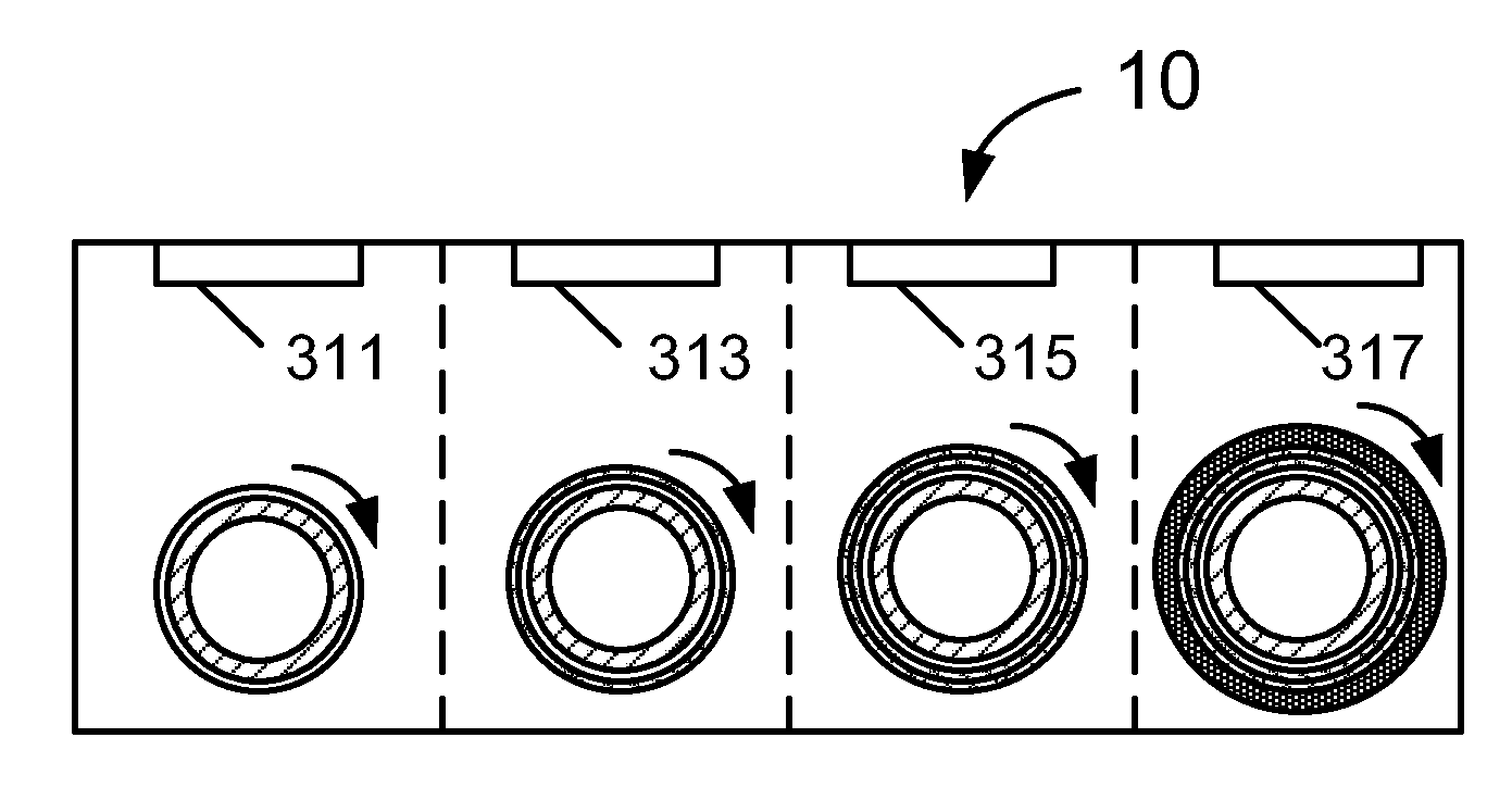
[0019]FIG. 1 is a simplified flowchart illustrating a method of fabricating a thin film photovoltaic cell including in-chamber sodium doping according to an embodiment of the present invention. This diagram is merely an example, which should not unduly limit the scope of the claims herein. The method 1000 includes the following processes:

[0020]1. Process 1010 for providing a shaped substrate member having a surface region in a first cha...


PUM

PropertyMeasurementUnit
temperatureaaaaaaaaaa
thicknessaaaaaaaaaa
temperatureaaaaaaaaaa

Abstract

A method of sodium doping in fabricating CIGS / CIS based thin film solar cells includes providing a shaped substrate member. The method includes forming a barrier layer over the surface region followed by a first electrode layer, and then a sodium bearing layer. A precursor layer of copper, indium, and / or gallium materials having an atomic ratio of copper / group III species no greater than 1.0 is deposited over the sodium bearing layer. The method further includes transferring the shaped substrate member to a second chamber and subjecting it to a thermal treatment process within an environment comprising gas-phase selenium species, followed by an environment comprising gas-phase sulfur species with the selenium species being substantially removed to form an absorber layer.

Description

CROSS-REFERENCE TO RELATED APPLICATION[0001]This application claims priority to U.S. Provisional Patent Application No. 61 / 176,857, filed May 8, 2009, entitled “SODIUM DOPING METHOD AND SYSTEM FOR SHAPED CIGS / CIS BASED THIN FILM SOLAR CELLS” by inventors Robert D Wieting, Steven Aragon, and Chester A. Farris III., commonly assigned and incorporated by reference herein for all purposes.BACKGROUND OF THE INVENTION[0002]This invention relates generally to photovoltaic techniques. More particularly, embodiments of the present invention provide a method and system for sodium doping in fabricating a copper indium diselenide species (CIS), copper indium gallium diselenide species (CIGS) based thin film photovoltaic cell, as well as other types of cells. The invention can be applied to various shaped cells including cylindrical / tubular photovoltaic modules, non-planar surfaces, flexible sheets, plastics, building or window glass, roof tiles, automobiles, and others.[0003]In the process of m...

Claims


Application Information

Patent Timeline
Patent Type & Authority Patents(United States)
IPC IPC(8): H01L21/00H01L31/00
CPCH01L31/03923H01L31/0749H01L31/0322Y02E10/541
Inventor WIETING, ROBERT D.ARAGON, STEVENFARRIS, III, CHESTER A.
Owner CM MFG
Why Eureka
Try Eureka