
Partially patterned lead frames and methods of making and using the same in semiconductor packaging

a technology of lead frame and patterned frame, which is applied in the field of semiconductor packaging, can solve the problems of handling flaws, affecting the structural rigidity of conventional lead frame, and affecting the stability of semiconductor packaging, so as to achieve the effect of improving structural rigidity

Inactive Publication Date: 2012-08-07
UNISEM M BERHAD
View PDF84 Cites 21 Cited by
  • Summary
  • Abstract
  • Description
  • Claims
  • Application Information

AI Technical Summary

Benefits of technology

The partially patterned lead frame enhances manufacturing efficiency, reduces gold wire usage, improves bond quality, and simplifies the packaging process by providing structural integrity and flexibility, while also accommodating complex device designs and reducing production costs.

Problems solved by technology

Conventional lead frames generally lack structural rigidity.
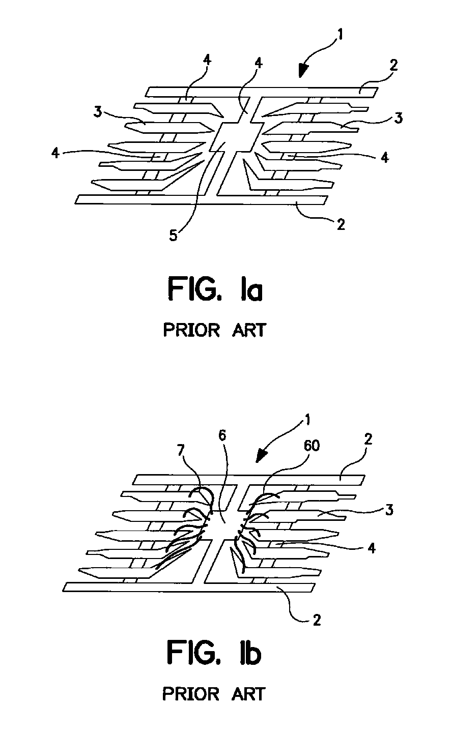
The finger-like portions of lead frames can be quite flimsy and difficult to hold in position.
This leads to handling flaws, damage and distortion in assembly processes and complicated wire bonding situations.
A failure to optimize the bonding parameters to compensate for the mechanical instability of the lead frame can result in poor bond adhesion, and hence poor quality and poor reliability of the bond.
The prior art has not shown any lead frames that can withstand the stresses encountered in current semiconductor packaging processes and that can be manufactured in a cost effective manner.
The need for longer wires can cause wire sway during processing and can potentially make certain types of chip scale packages prone to wire shorting.
Increasing wire length also affects unit cost.
The price of gold has virtually tripled in the last five years, and as the chip size decreases, the amount of gold wire increases, causing significant pricing pressure on chip package manufacturers.
Although coated wires are an alternative to gold wires, they are 2-3 times more expensive.
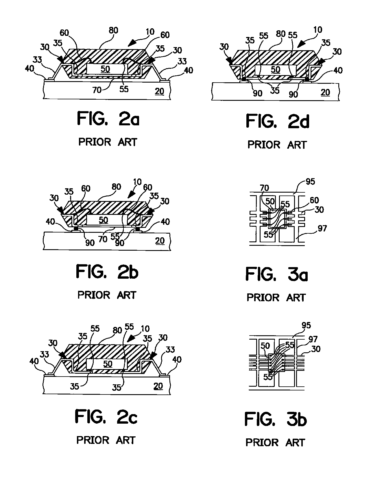
Laminated devices commonly have such RF shielding, but it is a very costly feature.
However, multiple passes with a saw can affect productivity and production yield.

Method used


Image

  • Partially patterned lead frames and methods of making and using the same in semiconductor packaging
  • Partially patterned lead frames and methods of making and using the same in semiconductor packaging
  • Partially patterned lead frames and methods of making and using the same in semiconductor packaging

Examples


Embodiment Construction

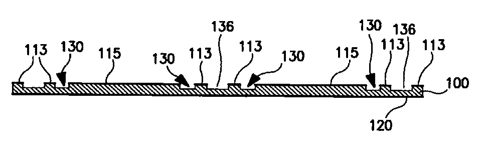
[0161]The present invention will now be described with reference to the Figures, wherein like numeral refer to like elements, FIGS. 4-15b and FIGS. 16-24b show different embodiments of forming a partially patterned lead frame package with lead counts comparable to that of near-chip scale packages (CSPs). The method of the invention improves the automation of the manufacturing line and the quality and reliability of the packages made therefrom. This is accomplished by performing a major portion of the manufacturing process steps with a partially patterned metal film formed into a web-like lead frame on one side. In contrast with conventionally punched through stencil-like lead frames, the lead frame used in the invention is partially patterned on one side and is solid and flat on the other side. This construction is improved both mechanically and thermally, and performs without distortion or deformation during the chip-attach, wire bond, and encapsulation processes. The bottom surfac...


PUM


Abstract

A method of making a lead frame and a partially patterned lead frame package with near-chip scale packaging lead-count, wherein the method lends itself to better automation of the manufacturing line and improved quality and reliability of the packages produced therefrom. A major portion of the manufacturing process steps is performed with a partially patterned strip of metal formed into a web-like lead frame on one side so that the web-like lead frame is also rigid mechanically and robust thermally to perform without distortion or deformation during the chip-attach and wire bond processes, both at the chip level and the package level. The bottom side of the metal lead frame is patterned to isolate the chip-pad and the wire bond contacts only after the front side, including the chip and wires, is hermetically sealed with an encapsulant. The resultant package being electrically isolated enables strip testing and reliable singulation.

Description

[0001]This application is a continuation-in-part of U.S. patent application Ser. No. 12 / 875,248, filed Sep. 3, 2010, which is a continuation of application Ser. No. 11 / 877,732, filed Oct. 24, 2007, now U.S. Pat. No. 7,790,500, which is a continuation-in-part of application Ser. No. 11 / 553,664, filed Oct. 27, 2006, now U.S. Pat. No. 7,799,611, which is a continuation-in-part of application Ser. No. 11 / 197,944, filed Aug. 4, 2005, now U.S. Pat. No. 7,622,332, which is a continuation of application Ser. No. 10 / 916,093, filed Aug. 10, 2004, now U.S. Pat. No. 7,129,116, which is a continuation of application Ser. No. 10 / 134,882, filed Apr. 29, 2002, now U.S. Pat. No. 6,812,552. All of these applications are incorporated herein by reference in their entirety.FIELD OF THE INVENTION[0002]The invention relates to electronic packaging in general, and more particularly, to a partially patterned lead frame and a method for making and using the same. The partially patterned lead frame is stronge...

Claims


Application Information

Patent Timeline
Patent Type & Authority Patents(United States)
IPC IPC(8): H01L21/50
CPCH01L21/4832H01L21/561H01L21/6835H01L23/49524H01L23/49548H01L23/552H01L24/12H01L24/32H01L24/40H01L24/49H01L24/73H01L24/91H01L24/97H01L25/0657H01L23/3107H01L24/28H01L24/29H01L24/45H01L2221/68331H01L2221/68377H01L2224/13099H01L2224/16245H01L2224/2919H01L2224/32057H01L2224/32145H01L2224/32245H01L2224/45014H01L2224/45124H01L2224/45144H01L2224/45147H01L2224/48091H01L2224/48145H01L2224/48227H01L2224/48247H01L2224/48257H01L2224/48465H01L2224/49171H01L2224/49175H01L2224/49433H01L2224/73265H01L2224/83385H01L2224/83855H01L2224/85439H01L2224/85444H01L2224/92247H01L2224/97H01L2225/0651H01L2225/06568H01L2924/01002H01L2924/01005H01L2924/01013H01L2924/01028H01L2924/01029H01L2924/0103H01L2924/01046H01L2924/01047H01L2924/01049H01L2924/0105H01L2924/01051H01L2924/01075H01L2924/01078H01L2924/01079H01L2924/01082H01L2924/01083H01L2924/014H01L2924/0781H01L2924/14H01L2924/15311H01L2924/19041H01L2924/19043H01L2924/19105H01L2924/3025H01L24/48H01L2924/01006H01L2924/01033H01L2924/01044H01L2924/01045H01L2924/0132H01L2924/0133H01L2224/291H01L2924/15747H01L2224/29111H01L2224/32257H01L2224/73221H01L2924/07802H01L2224/26175H01L2924/00014H01L2224/85H01L2224/83H01L2924/0665H01L2224/81H01L2924/00012H01L2924/00H01L2224/45015H01L2924/351H01L2924/181H01L2224/48639H01L2224/48839H01L2224/48844H01L2224/48644H01L2224/48739H01L2224/48744H01L2224/40245H01L2224/05554H01L2224/371H01L2224/37147H01L2224/8385H01L2224/37139H01L2224/3754H01L24/37H01L2224/8485H01L2224/84801H01L2224/83101H01L24/16H01L24/83H01L2224/85205H01L2224/13147H01L2224/13082H01L24/84H01L2224/06131H01L2924/20752H01L2924/00015H01L2924/206
Inventor SAN ANTONIO, ROMARICO S.MCKERREGHAN, MICHAEL H.SUBAGIO, ANANGTORIAGA, ALLAN C.
Owner UNISEM M BERHAD
Learn More