Gate drive device

a drive device and gate technology, applied in the field of gate drive devices, can solve the problems of inability to utilize the effect of low-pass filtering, inability to use the effect of low-pass filter, and decrease the reliability of active elements, so as to prevent the flow out of the capacity, and suppress the sudden change in output voltage

Active Publication Date: 2012-07-10
FUJI ELECTRIC CO LTD
View PDF40 Cites 6 Cited by
  • Summary
  • Abstract
  • Description
  • Claims
  • Application Information

AI Technical Summary

Benefits of technology

[0023]In view of the foregoing, the invention, being conceived bearing in mind the unsolved problems of the above-described known example, has an object of providing a gate drive device which can suppress the fluctuation of an internal power source voltage and output voltage, while reducing the number of parts by omitting a bypass capacitor connected in parallel with a semiconductor integrated circuit.
[0024]In order to achieve the above-described object, a gate drive device according to one aspect of the invention, which drives the gate of an active element with a large input capacity such as an IGBT or MOSFET, includes a semiconductor integrated circuit, which has an internal power source circuit forming an internal power source based on an external power source supplied from an external power source such as a battery. The semiconductor integrated circuit incorporates a voltage drop suppressing circuit. The voltage drop suppressing circuit, when an input power source voltage of the external power source momentarily drops below a minimum operating voltage, prevents a drop of an internal power source voltage of the internal power source circuit below the minimum operating voltage, and a steep drop in a voltage output to the gate.
[0028]Also, the gate drive device according to the aspect of the invention is configured so that the switching element is configured of, e.g., comprises, an N-type MOSFET. A control voltage which has a fall time sufficiently short in comparison with the drop time for which the external power source voltage and internal power source voltage drop below the minimum operating voltage, and a rise time sufficiently long in comparison with the drop time, is applied to the gate of the N-type MOSFET. According to this configuration, when the power source voltage drops below the minimum operating voltage, the N-type MOSFET is put into a turned off condition in a short time, and a flowing out of a charge accumulated at the gate of the active element is prevented.
[0031]Put in other terms, embodiments of the invention relate to a gate drive device that can comprise a semiconductor integrated circuit, connected to an internal power source circuit supplied by an external power source. The gate drive device can further comprise a voltage drop suppressing circuit configured to, if an external power source voltage corresponding to the external power source drops below a minimum operating voltage, prevent a drop of an internal power source voltage corresponding to the internal power source circuit below the minimum operating voltage. The voltage drop suppressing circuit can further be configured to prevent a drop of at least a predetermined magnitude in a voltage output to a gate of the gate drive device.
[0035]According to this configuration, when a voltage drop in the power source voltage input into the semiconductor integrated circuit, or in the internal power source voltage, is detected in the undervoltage detection circuit, it is possible to suppress a sudden change in the output voltage by controlling the second N-type MOSFET into a turned off condition, and to prevent the flowing out of the capacity accumulated at the gate of the active element.
[0036]According to the invention, when the gate of an active element with a large capacity such as an IGBT or power MOSFET is driven by a gate drive device, a voltage drop suppressing circuit is incorporated in a semiconductor integrated circuit and, when an input power source voltage momentarily drops below a minimum operating voltage, a drop of an internal power source voltage of the internal power source circuit below the minimum operating voltage, and a sharp drop in a voltage output to the gate, are prevented by the voltage drop suppressing circuit. Additionally, the voltage drop suppressing circuit supplies a minimum current at which the circuit connected to the internal power source can operate during the voltage drop period. For this reason, an advantage is obtained wherein it is possible to prevent at least one of the internal power source voltage and output voltage of the semiconductor integrated circuit from momentarily dropping below the minimum operating voltage of the semiconductor integrated circuit, while reducing the number of parts by omitting a bypass capacitor inserted in parallel with the semiconductor integrated circuit.

Problems solved by technology

Also, in the event that a high, abnormal current higher than the normal current flows through an active element such as an IGBT or MOSFET, the voltage between the gate and emitter of the active element rises, due to which a collector current increases, and the reliability of the active element decreases.
However, when omitting the bypass capacitor C2 with the object of reducing the number of parts, it becomes impossible to utilize the effect of the low pass filter.
In the face of this kind of steep voltage drop, it is not possible either to obtain a sufficient advantage from the method described in JP-A-2-7714, whereby the voltage between the gate and emitter of the IGBT is clamped.

Method used


Image

  • Gate drive device
  • Gate drive device
  • Gate drive device

Examples


first embodiment

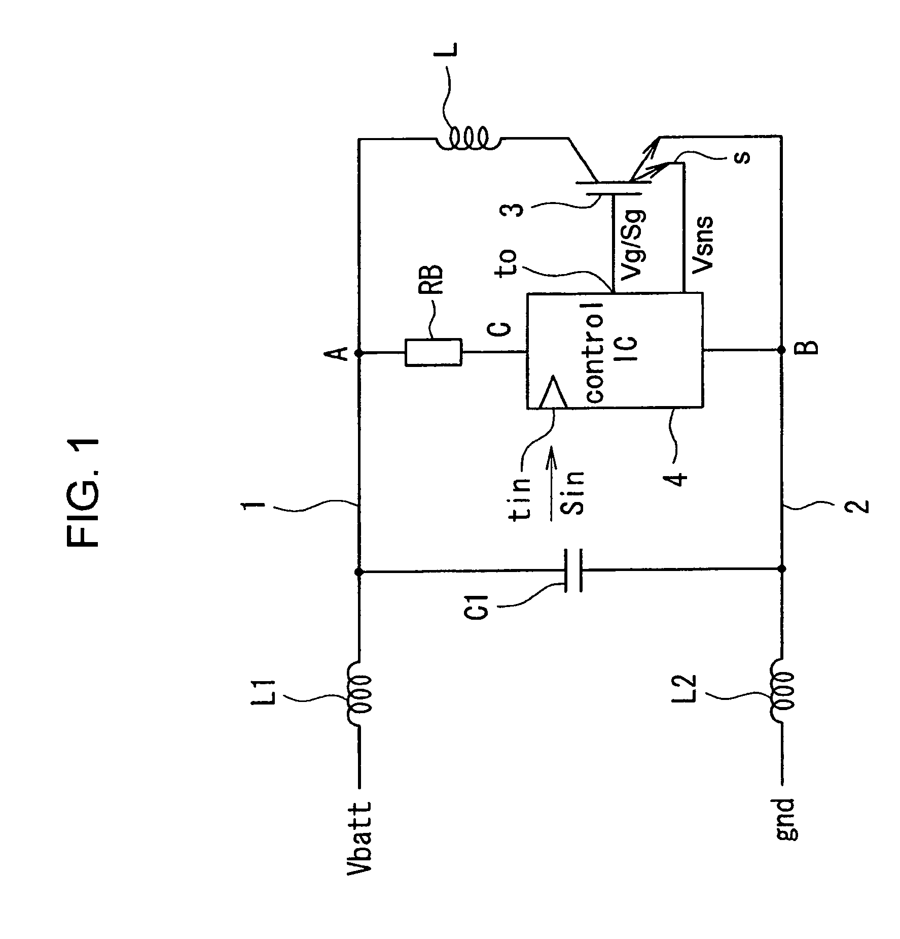
[0047]FIG. 1 is a circuit diagram showing the invention. The circuit shown in FIG. 1 has the same configuration as the configuration of the circuit of FIG. 6, which shows the previously described known example, except that the bypass capacitor C2 is omitted.

[0048]As shown in FIG. 1, an inductor L acting as a load, and an IGBT 3 acting as a large capacity active element, are connected in series between a power source line 1, to which a battery voltage Vbatt is applied from a battery acting as a power source, and a ground line 2 connected to a ground gnd.

[0049]The gate of the IGBT 3 is driven by a control IC 4 configured of, e.g., comprising, a semiconductor integrated circuit. The power source input side of the control IC 4 is connected at a connection point A to the power source line 1 via a current limiting resistor RB, and the ground side is connected to the ground line 2 at a connection point B.

[0050]Also, the control IC 4 is configured so that, as well as a control signal Sin be...

second embodiment

[0073]Next, a description will be given, based on FIGS. 4 and 5, of the invention.

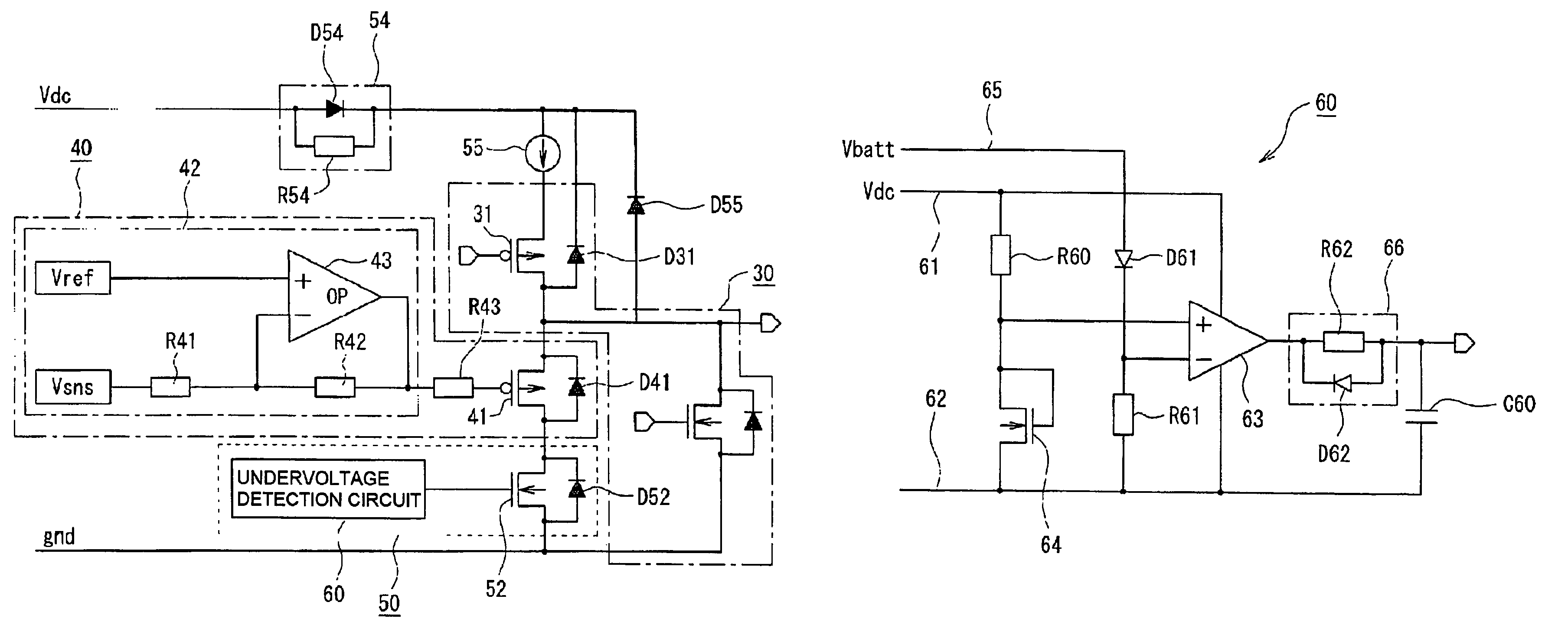
[0074]In the second embodiment, the self-biasing circuit is omitted, and an undervoltage detection circuit is applied in its place.

[0075]That is, the second embodiment has the same configuration as the first embodiment of FIG. 2, except that a normal constant current circuit 55 is applied in place of the second P-type MOSFET 51 of the first embodiment, and that the gate of the N-type MOSFET 52 is driven by an undervoltage detection circuit 60, as shown in FIG. 4. Consequently, the same reference numerals and characters are given to portions corresponding to those in FIG. 2, and a detailed description thereof is omitted.

[0076]Herein, the undervoltage detection circuit 60, being able to respond to a steep voltage fluctuation and having a circuit configuration capable of a low power source voltage operation, is configured as shown in FIG. 5. That is, the undervoltage detection circuit 60 includes a self-b...


PUM


Abstract

A gate drive device which can suppress the fluctuation of an internal power source voltage and output voltage, while reducing the number of parts by omitting a bypass capacitor connected in parallel with a semiconductor integrated circuit, is provided. The gate drive device drives the gate of an active element with a large input capacity, such as an IGBT or MOSFET, and includes a semiconductor integrated circuit. The semiconductor integrated circuit has an internal power source based on an external power source, such as a battery. The semiconductor integrated circuit incorporates a voltage drop suppressing circuit, configured so that, if an input external power source voltage momentarily drops below a minimum operating voltage, a drop of an internal power source voltage below the minimum operating voltage, and a sharp drop in a voltage output to the gate, are prevented by the voltage drop suppressing circuit.

Description

CROSS-REFERENCE TO RELATED APPLICATIONS[0001]This application claims priority under 35 U.S.C. §119 from JP PA 2009-116445, filed May 13, 2009, the entirety of which is incorporated herein by reference.BACKGROUND OF THE INVENTION[0002]1. Technical Field[0003]The present invention relates to a gate drive device which drives the gate of an active element with a large input capacity, such as an insulated gate bipolar transistor (IGBT) or power metal oxide semiconductor field effect transistor (MOSFET).[0004]2. Related Art[0005]As this kind of gate drive device, there is known a gate drive circuit which drives the gate of an IGBT (for example, refer to JP-A-2000-59195).[0006]This gate drive circuit has a configuration wherein a P-type MOSFET, a supersaturation reactor, a diode, and an N-type MOSFET are connected in series between a voltage source and a ground. Then, a connection point between the P-type MOSFET and supersaturation reactor is connected via a gate protection resistor to the...

Claims


Application Information

Patent Timeline
Patent Type & Authority Patents(United States)
IPC IPC(8): H03K17/14
CPCH03K17/0828H03K17/162H03K17/165
Inventor KOHAMA, TAKANORIMASUZAWA, KAZUTAKAKUMAGAI, NAOKI
Owner FUJI ELECTRIC CO LTD
Why Eureka
Try Eureka