Three-dimensional LADAR module with alignment reference insert circuitry comprising high density interconnect structure

a high density, interconnecting structure technology, applied in the direction of reradiation, distance measurement, instruments, etc., can solve the problems of undesirable sensor types, lack of circuit speed and capacity to achieve very high resolution and sensitivity of centimeter range, etc., to achieve enhanced imaging capability, reduce layer-to-layer or channel-to-channel jitter, and increase detector output processing circuit density

Active Publication Date: 2012-06-12
AI CORE TECH LLC
View PDF34 Cites 17 Cited by
  • Summary
  • Abstract
  • Description
  • Claims
  • Application Information

AI Technical Summary

Benefits of technology

[0017]In yet a further aspect of the invention, one or more alignment reference points are inserted at a predetermined point in the image capture cycle to allow the electronic alignment of selected sets of image data collected by the FIFO shift registers in the one or more channels of the one or more ROICs contained in the processing module. In this aspect of the invention, alignment reference point insertion and alignment circuitry is provided as means to minimize layer-to-layer or channel-to-channel “jitter” which may be present due to variances in layer operating or data capture start-up characteristics. Alternatively, the invention allows a user to selectively insert an alignment reference point in an individual channel.
[0018]The enhanced imaging capability provided by the claimed invention is achieved, in part, by the use of stacked layers containing the ROIC circuitry, which increases detector output processing circuit density while minimizing circuit lead length and associated electrical parasitics. The benefit of the use of stacked layers of ROIC circuitry is the ability to integrate a large (e.g., 128×128 or larger) detector array with associated dedicated detector readout circuitry (amplifier, threshold detector, sampling circuitry, analog to digital (ADC), digital to analog converters (DAC) and first in, first out, (FIFO) shift register “range” bins all within a very small module.

Problems solved by technology

Unfortunately, existing LADAR imaging systems lack the necessary circuit speed and capacity to achieve very high (i.e., centimeter) range resolution and sensitivity.
Nonetheless, these types of sensors are undesirable where accurate scene information in a complex video environment (i.e., camouflaged or partially obscured targets) is an important factor in the observer's decision-making.

Method used


Image

  • Three-dimensional LADAR module with alignment reference insert circuitry comprising high density interconnect structure
  • Three-dimensional LADAR module with alignment reference insert circuitry comprising high density interconnect structure
  • Three-dimensional LADAR module with alignment reference insert circuitry comprising high density interconnect structure

Examples


Embodiment Construction

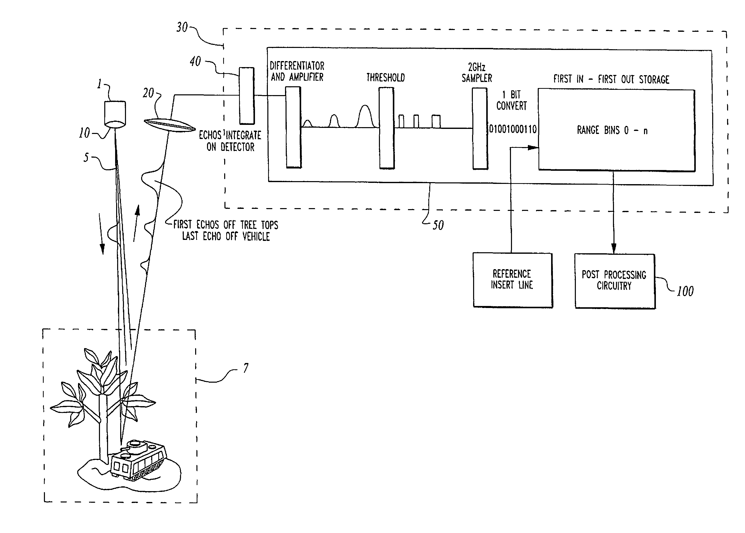
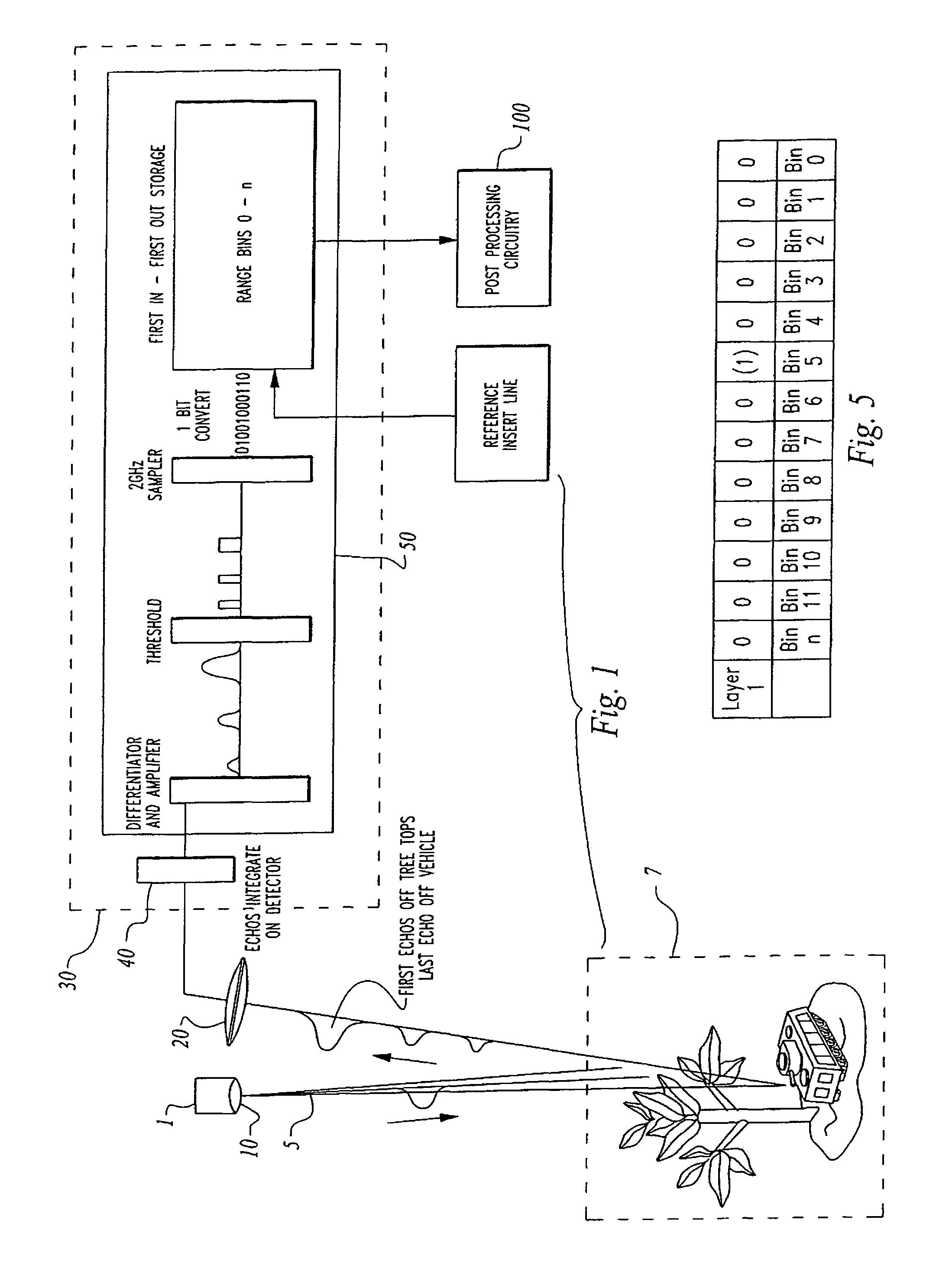
[0040]Turning now to the figures wherein like numerals designate like elements among the several views, FIG. 1 shows a block diagram of a preferred embodiment of the present invention.

[0041]A photon source, such as a laser 1, generates a beam pulse 5, which is directed toward a scene or target 7, through suitable beam-shaping optics 10.

[0042]A 3-D LADAR imaging system incorporating stacked microelectronic layers is provided. A light source such as a laser is imaged upon a target through beam shaping optics. Photons reflected from the target are collected and imaged upon a detector array through collection optics. The detector array signals are fed into a multilayer processing module Wherein each layer includes detector signal processing circuitry. The detector array signals are amplified, compared to a user-defined threshold, digitized and fed into a high speed FIFO shift register range bin. Dependant on the value of the digit contained in the bins in the register, and the digit's b...


PUM


Abstract

A 3-D LADAR imaging system incorporating stacked microelectronic layers is provided. A reference insert circuit inserts data into the FIFO registers at a preselected location to provide a reference point at which all FIFO shift register data may be aligned to accommodate for timing differences between layers and channels. The bin data representing the photon reflections from the various target surfaces are read out of the FIFO and processed using appropriate circuitry such as a field programmable gate array to create a synchronized 3-D point cloud for creating a 3-D target image.

Description

CROSS REFERENCE TO RELATED APPLICATIONS[0001]This application is a continuation-in-part of U.S. patent application Ser. No. 11 / 499,403, entitled “High Density Interconnect Assembly Comprising Stacked Electronic Module,” filed Aug. 4, 2006, which claims priority to and the benefit of U.S. Provisional Patent Application No. 60 / 711,375, entitled “High Density Interconnect Scheme For Stacked Electronic Modules,” filed Aug. 26, 2005, each of which is incorporated herein by reference.[0002]This application is a continuation-in-part of U.S. patent application Ser. No. 11 / 706,724, entitled “Three Dimensional LADAR Module with Alignment Reference Circuitry,” tiled Feb. 15, 2007 (now U.S. Pat. No. 7,436,494), which claims priority to and the benefit of U.S. Provisional Patent Application No. 60 / 785,135, filed Mar. 24, 2006, entitled, “Method for Image Jitter Reduction in a Multilayer LADAR Device,” and is also a continuation-in-part of U.S. patent application Ser. No. 10 / 806,037, entitled “Th...

Claims


Application Information

Patent Timeline
Patent Type & Authority Patents(United States)
IPC IPC(8): G01C3/08
CPCG01S7/4816G01S7/486G01S7/4863G01S17/89H05K3/366H01L25/0657G01S17/10G01S17/42H01L24/29H01L2225/06551H01L2225/06596H01L2924/01004H01L2924/01005H01L2924/01079H01L2924/14H01L2924/1433H01L2924/19041H01L2924/19042H01L2924/19043H01L2924/30105H01L2924/30107H01L2224/45147H01L2924/00H01L2924/00014H01L2224/48G01S17/894H01L2224/45565H01L2224/45644
Inventor KENNEDY, JOHNLUDWIG, DAVIDKRUTZIK, CHRISTIAN
Owner AI CORE TECH LLC
Why Eureka
Try Eureka