Scanning electron microscope
a scanning electron microscope and microscope technology, applied in the field of scanning electron microscopes, can solve the problems of reducing measurement precision, insufficient measurement precision, and inability to obtain clear images with sufficient measurement precision, and achieve the effect of measuring precision
- Summary
- Abstract
- Description
- Claims
- Application Information
AI Technical Summary
Benefits of technology
Problems solved by technology
Method used
Image
Examples
first embodiment
[0025]The first embodiment of the present invention will now be described with reference to the drawings.
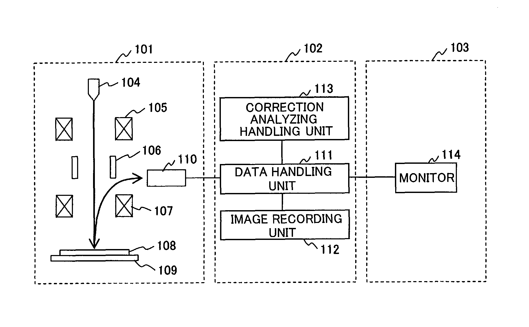
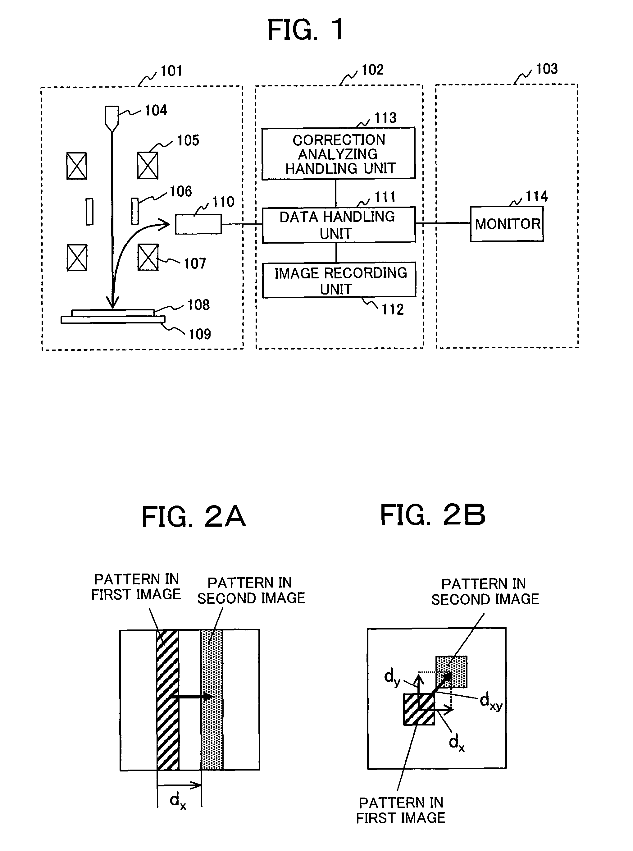
[0026]FIG. 1 shows an embodiment of a scanning electron microscope including a drift correction function. This apparatus makes it possible to acquire clear frame images by calculating a drift rate and correcting drift, even if the image drift occurs. The image drift is a phenomenon that the images shift with time at observation of a sample. In this description, the “drift rate” implies the amount of positional deviation (shift rate) of patterns between frame images shown in FIG. 2 and also the shift rate between field images.
[0027]The scanning electron microscope including an image correction function includes an electron microscope unit 101, a control unit 102, and a display unit 103. An electron beam emitted from an electron source 104 is focused by a condenser lens 105 and an objective lens 107, then irradiated onto a sample 108. The electron beam is scanned two-dimensionally ...
second embodiment
[0057]Descriptions will now be made of the second embodiment using FIG. 10 and FIG. 11. The contents of the first embodiment are applicable also to this embodiment, unless special circumstances are present.
[0058]FIG. 10 is a flowchart showing the process of this embodiment. Descriptions will now be made of this flowchart.
[0059]The stage is moved to an observation point. Then, plural one-frame images are continuously acquired in the same field. The frame images thus acquired are stored in the image recording unit 112 (S1001).
[0060]The correction analyzing handling unit 113 is used for reducing the frame images so as to improve the S / N ratio (S1002).
[0061]The correction analyzing handling unit 113 is used for judging whether the pattern is one-dimensional or two-dimensional, using Computer Aided Design (CAD) data as design data corresponding to the target pattern to be observed or frame image data which has been acquired through the observation. In addition, an applicable analyzing me...
third embodiment
[0072]Descriptions will now be made of the third embodiment of the present invention. The contents of the first embodiment are applicable also to this embodiment, unless special circumstances are present.
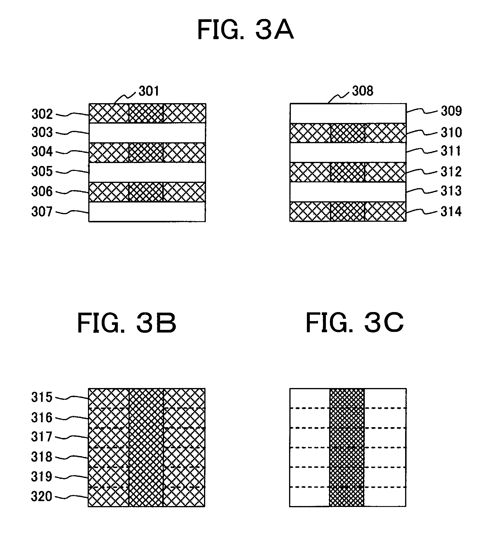
[0073]In the first embodiment, the drift rate of each frame has been obtained, and the obtained drift rate is divided into the number of field images, so as to perform drift correction. In this technique, the calculation of the drift rate is made by comparing the one-frame images. However, the drift rate cannot be obtained with high accuracy between the one-frame images as they are when the S / N ratio is remarkably low. In consideration of this, according to one technique, correction is performed by superimposing plural one-frame images so as to form a new image, and obtaining a drift rate between these images with an improved S / N ratio. The minimum number of one-frame images to be superimposed is set so that an S / N ratio capable of obtaining the drift rate is obtained. In this case,...
PUM
 Abstract
Description
Claims
Application Information
 - R&D
- Intellectual Property
- Life Sciences
- Materials
- Tech Scout
- Unparalleled Data Quality
- Higher Quality Content
- 60% Fewer Hallucinations
Browse by: Latest US Patents, China's latest patents, Technical Efficacy Thesaurus, Application Domain, Technology Topic, Popular Technical Reports.
© 2025 PatSnap. All rights reserved.Legal|Privacy policy|Modern Slavery Act Transparency Statement|Sitemap|About US| Contact US: help@patsnap.com


