Method for forming thin film, substrate having transparent electroconductive film and photoelectric conversion device using the substrate
a technology of electroconductive film and substrate, which is applied in the direction of coating, chemical vapor deposition coating, semiconductor devices, etc., can solve the problems of difficult to obtain a uniform film thickness, low thermal deposition rate of thin film containing metal oxide, and inability to achieve uniform film thickness, etc., to achieve low reactivity and low deposition rate
- Summary
- Abstract
- Description
- Claims
- Application Information
AI Technical Summary
Benefits of technology
Problems solved by technology
Method used
Image
Examples
example 1
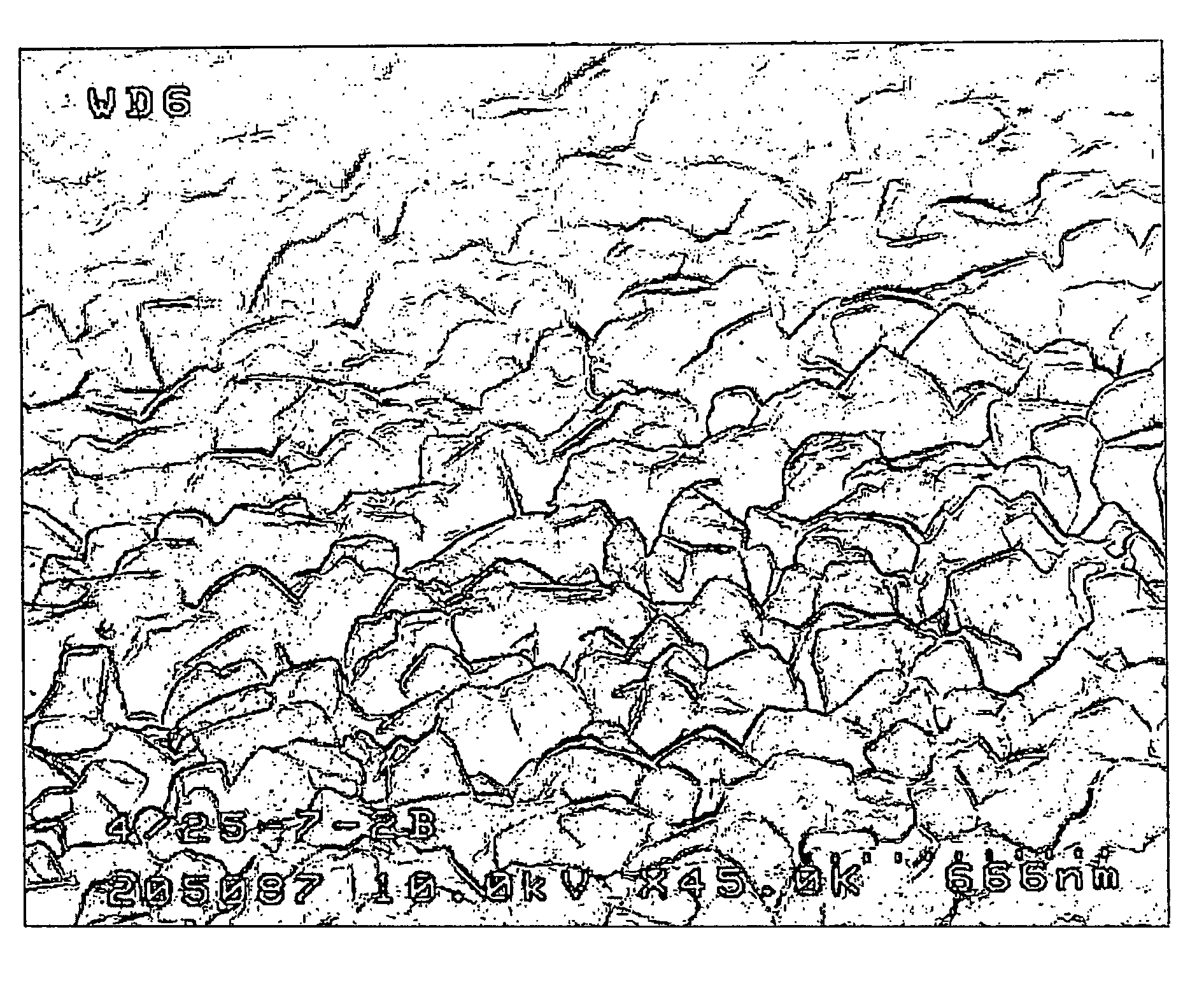
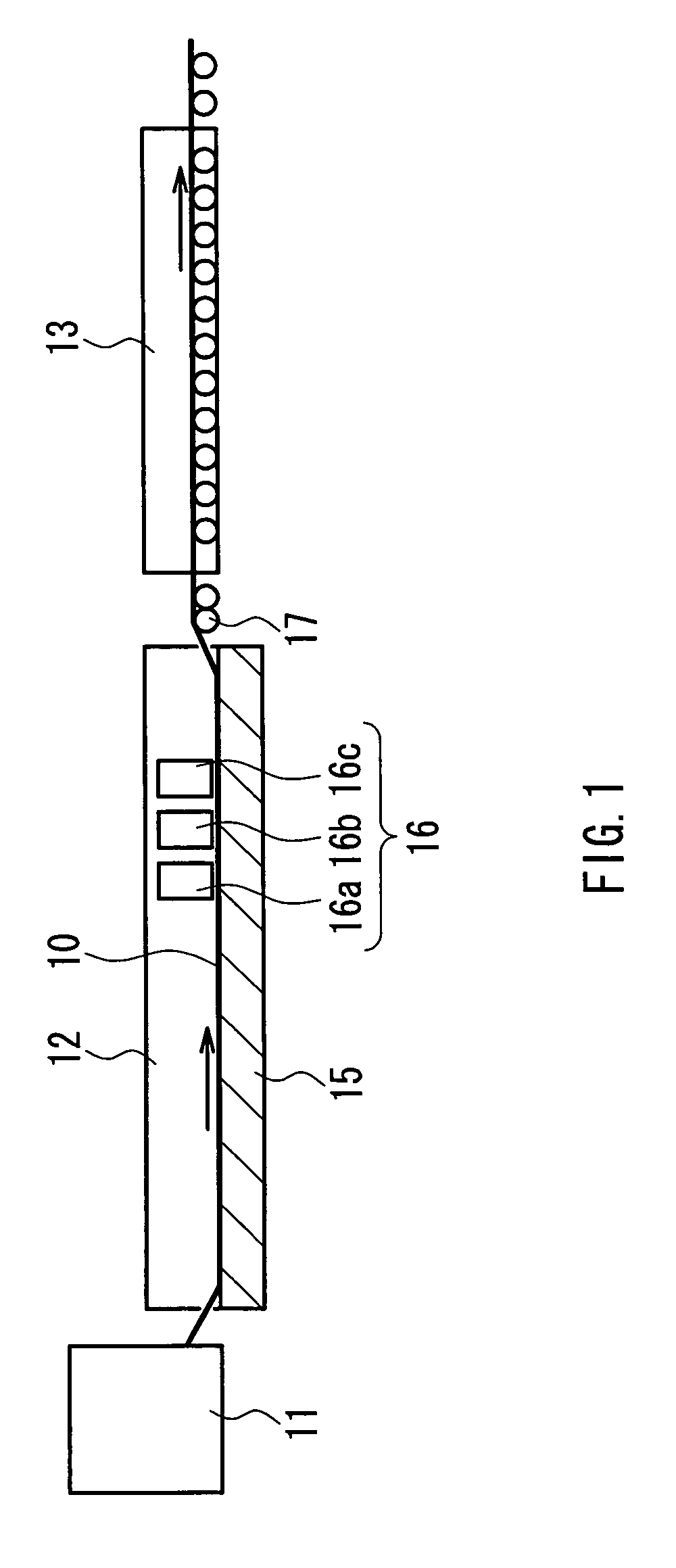
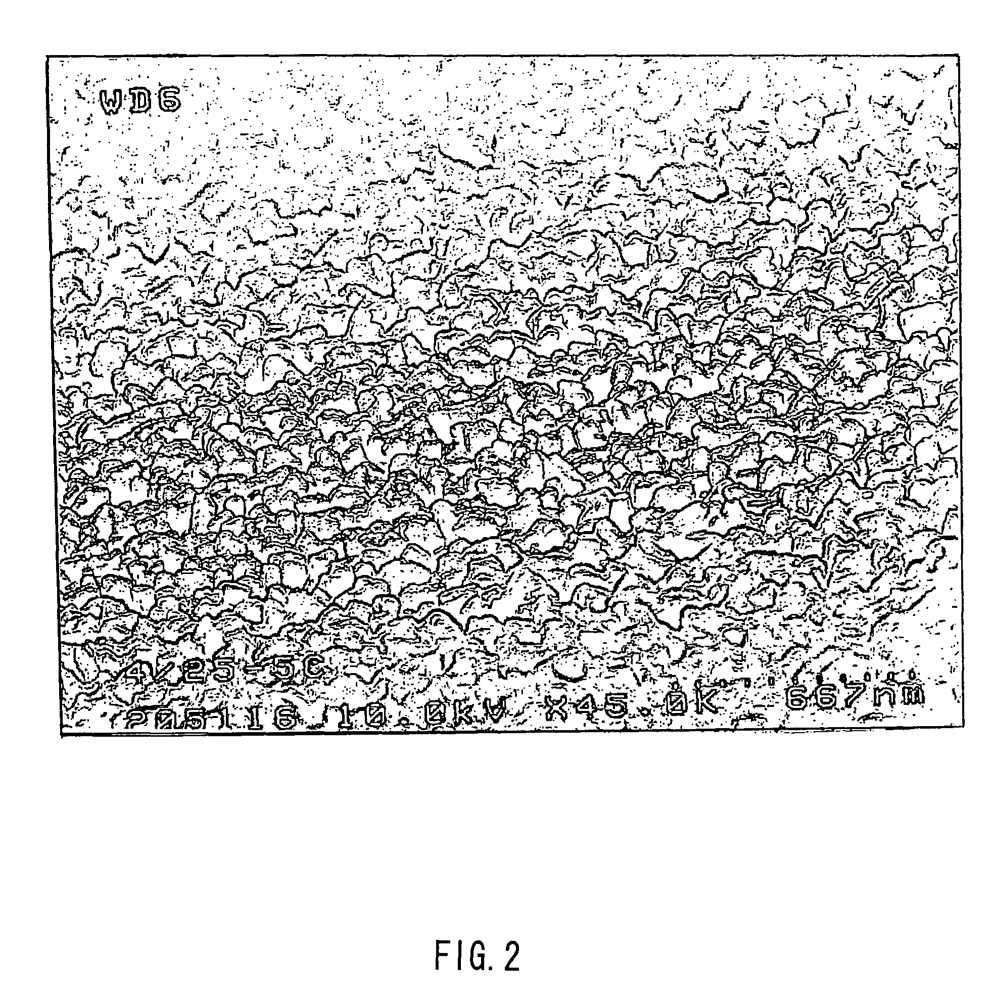
[0074]A 4-mm thick soda lime glass sheet that was cut into a size of 150×150 mm was placed on a mesh belt and was passed through a heating furnace to be heated to about 600° C. While transferring the heated glass sheet further, a mixed gas composed of monosilane, oxygen, and nitrogen was supplied from a coater installed above the transfer line to form a thin film (undercoating film) having a film thickness of 25 nm and composed of silicon oxide on the glass sheet. After annealing the glass sheet, the glass sheet was again placed on the mesh belt and passed through the heating furnace to be heated to about 620° C. While transferring the heated glass sheet further, a mixed gas composed of tin tetrachloride (vapor), oxygen, water vapor, and nitrogen was supplied from a coater installed above the transfer line to form a thin film (metal-containing thin film) having a film thickness of 30 nm and composed of tin oxide (SnO2) on the undercoating film at a film deposition rate of 50 nm / min....
example 2
[0076]A transparent conductive film was deposited in a similar manner to Example 1 except that the following points were changed, and the glass sheet was evaluated. The thickness of the undercoating film was changed to 20 nm; as for the metal-containing thin film, the thickness was changed to 100 nm and the film deposition rate to 160 nm / min; and as for the transparent conductive film, oxygen was added to the raw materials, the thickness was changed to 710 nm, and the film deposition rate was changed to 470 nm / min.
[0077]This glass sheet had a haze ratio of 17% and showed no white turbidity.
example 3
[0078]A transparent conductive film was deposited in a similar manner to Example 1 except that the following points were changed, and the glass sheet was evaluated. As the glass sheet, an aluminosilicate glass that does not contain alkaline components was used; and as for the metal-containing thin film, using as a metal chloride titanium chloride (vapor) for the raw material, a thin film having a thickness of 20 nm and composed of titanium oxide was formed at a film deposition rate of 30 nm / min. As for the transparent conductive film, oxygen and methyl alcohol were added to the raw materials; the thickness was changed to 900 nm and the film deposition rate was changed to 1000 nm / min.
[0079]This glass sheet had a haze ratio of 29% but showed no white turbidity.
PUM
| Property | Measurement | Unit |
|---|---|---|
| thickness | aaaaa | aaaaa |
| thickness | aaaaa | aaaaa |
| deposition rate | aaaaa | aaaaa |
Abstract
Description
Claims
Application Information
 - R&D
- Intellectual Property
- Life Sciences
- Materials
- Tech Scout
- Unparalleled Data Quality
- Higher Quality Content
- 60% Fewer Hallucinations
Browse by: Latest US Patents, China's latest patents, Technical Efficacy Thesaurus, Application Domain, Technology Topic, Popular Technical Reports.
© 2025 PatSnap. All rights reserved.Legal|Privacy policy|Modern Slavery Act Transparency Statement|Sitemap|About US| Contact US: help@patsnap.com


