Generation of a low jitter clock signal

a clock signal and low jitter technology, applied in the direction of electrical instruments, electric digital data processing, electrical equipment, etc., can solve the problems of affecting the desired rf signal output of the chip, and the distortion of the clock signal, so as to reduce reduce the transition time of the clock signal. , the effect of reducing the common impedance of the conducting path

Inactive Publication Date: 2011-12-27
ST ERICSSON SA
View PDF2 Cites 0 Cited by
  • Summary
  • Abstract
  • Description
  • Claims
  • Application Information

AI Technical Summary

Benefits of technology

[0011]Further, a common power supply is shared by the RF block, the digital block, and the LJC generator through a Kelvin connection. The Kelvin connection reduces common impedance of the conducting path of the power supply such that the jitters due to voltage fluctuations in the power supply are substantially reduced in the clock signals. The power supply is also shared between a radio frequency (RF) block and the DC-DC converter, again through the Kelvin connection. Therefore, voltage fluctuations coupled to the power supply are not coupled with the clock signals generated by the LJC generator, and thus generally do not distort the clock signals.
[0012]Moreover, the generated clock signals are passed through the receive buffer supplied with the common power supply, hereinafter referred to as LJC power supply, provided to the LJC generator. The receive buffer sharpens the edge rate of the clock signals such that the transition time of the clock signals is reduced to avoid introduction of noise in the clock signals due to coupling of the LJC power supply with the clock signals. Subsequently, the sharpened clock signals are driven to the wireless circuits through the clock buffer supplied with a power supply, hereinafter referred to as clock buffer power supply. On account of the clock signals being operated on with the LJC power supply and then with the clock buffer power supply of the wireless circuits, the coupling of the clock signals with the clock buffer power supply and the LJC power supply is reduced. As a result, introduction of noise in the clock signals due to coupling between the power supplies and the clock signals, which occurs in conventional systems, is substantially reduced.
[0015]In an embodiment, a method comprises: generating a clock signal; sharpening the clock signal to provide a sharpened clock signal; buffering the sharpened clock signal to provide a buffered clock signal; and providing the buffered clock signal to a wireless circuit. In an embodiment, sharpening the clock signal comprises increasing a rate of change of an edge of the clock signal.

Problems solved by technology

Although such an approach involving component sharing significantly reduces space constraints on the chip, the signals of the shared components can interfere with each other and with clock signals generated by the clock generator during operation of the chip.
This interference can be caused due to overlapping of noise from the analog and the digital blocks, both being directly or indirectly coupled to the clock generator through a common power supply, thereby causing distortion in the clock signals.
The distorted clock signals suffer from various imperfections, such as frequency drifts, phase shifts, and jitters, which adversely affect the desired RF signal output from the chip.
Generally, the shared conducting path of the common power supply contributes to large common impedance, due to which any fluctuation in current flowing through the current carrying blocks or the clock generator stimulates an unwanted phase shift in the clock signals.
As a result, frequent variations in the electrical state of the digital blocks introduce jitters in the clock signals due to coupling between the common power supply and the clock signals.
Moreover, a fluctuating power supply provided by a direct current-to-direct current (DC-DC) converter to various circuits, such as a clock divider circuit, may introduce jitters in the clock signals passing through these circuits due to capacitive and magnetic couplings between the clock signals and the applied power supply.

Method used


Image

  • Generation of a low jitter clock signal
  • Generation of a low jitter clock signal
  • Generation of a low jitter clock signal

Examples


Embodiment Construction

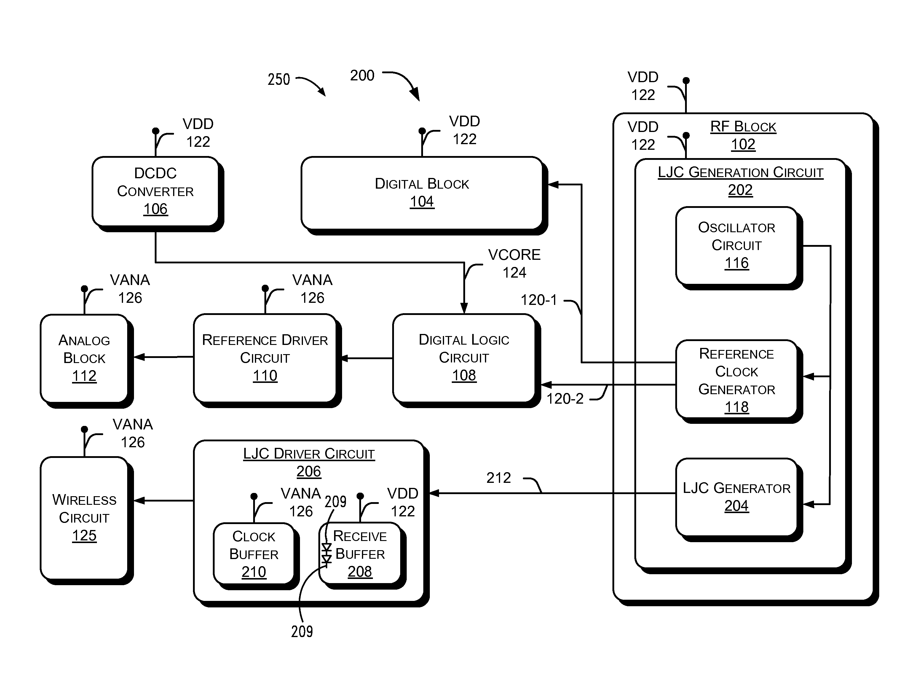
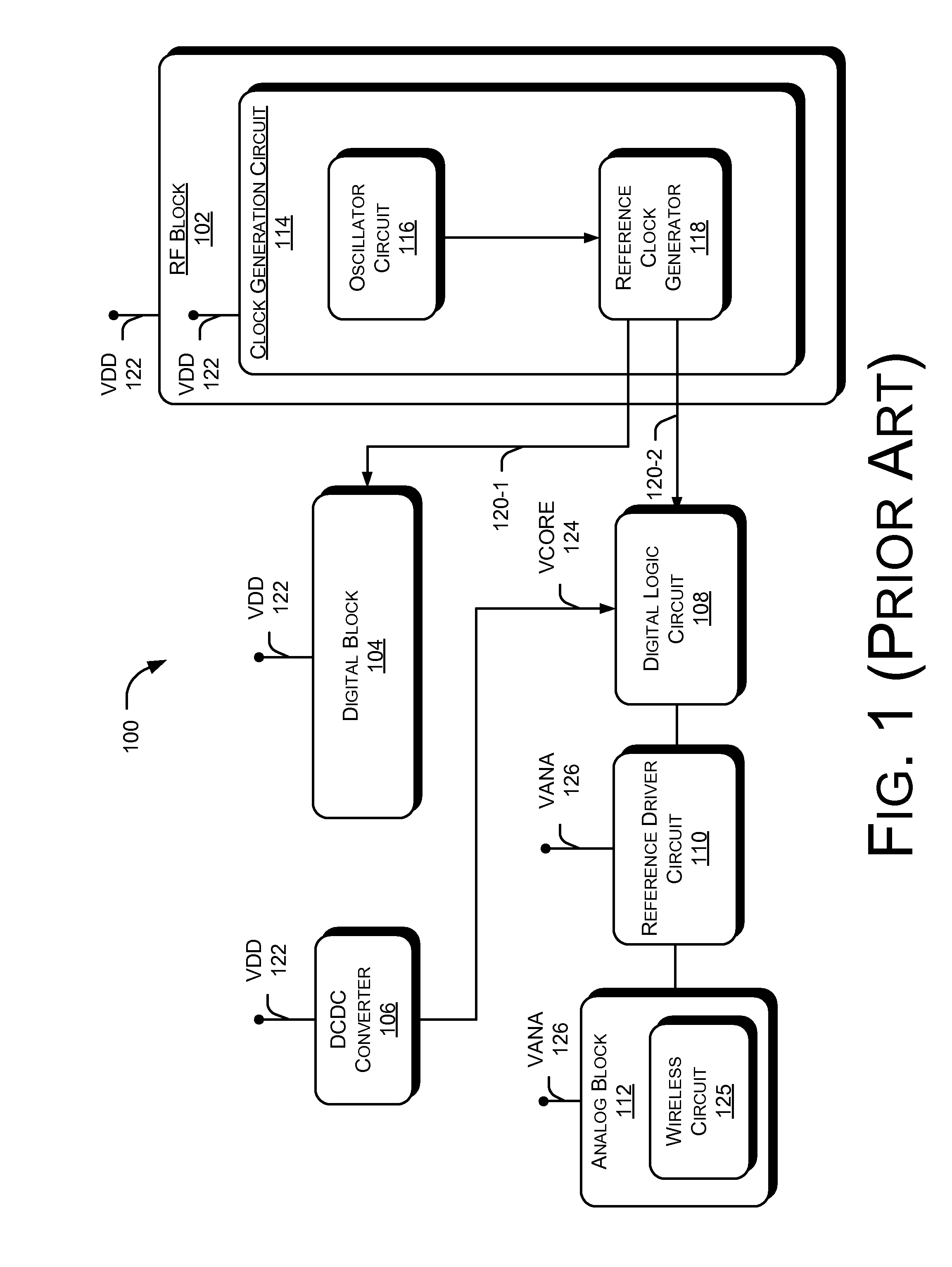
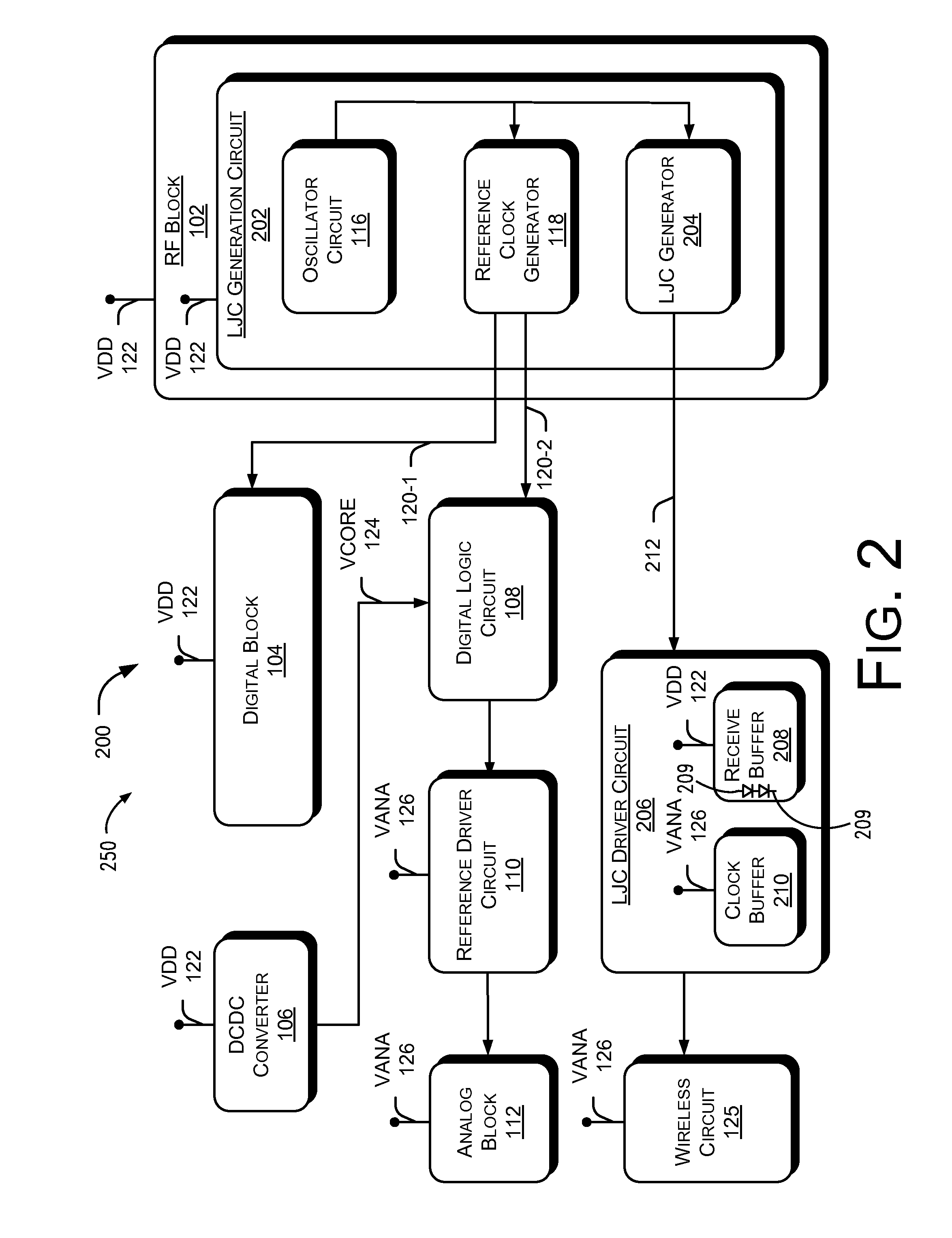
[0027]The disclosed subject matter relates to a system for generation of low jitter clock signals. More particularly, the subject matter relates to a system for providing a low jitter clock signal for wireless circuits, such as a Bluetooth circuit or a GPS circuit.

[0028]In the following description, numerous specific details are given to provide a thorough understanding of embodiments. The embodiments can be practiced without one or more of the specific details, or with other methods, components, materials, etc. In other instances, well-known structures, materials, or operations, such as, for example, power supplies, are not shown or described in detail to avoid obscuring aspects of the embodiments.

[0029]Reference throughout this specification to “one embodiment” or “an embodiment” means that a particular feature, structure, or characteristic described in connection with the embodiment is included in at least one embodiment. Thus, the appearances of the phrases “in one embodiment”“a...


PUM


Abstract

Systems and methods for generation of a low jitter clock signal for wireless circuits are disclosed. In an implementation, the system includes a wireless circuit powered by a first power supply and a low jitter clock (LJC) generator powered by a second power supply. The LJC generator provides at least one clock signal to the wireless circuit. The system further includes an LJC driver circuit including a clock buffer powered by the first power supply and a receive buffer powered by the second power supply.

Description

RELATED APPLICATION[0001]The present application claims priority of European Patent Application No. 09305184.5 filed Feb. 27, 2009.BACKGROUND[0002]1. Technical Field[0003]The disclosed subject matter relates to a system for generation of low jitter clock signals. More particularly, the subject matter relates to a system for providing a low jitter clock signal for wireless circuits, such as a Bluetooth circuit or a GPS circuit.[0004]2. Description of the Related Art[0005]Wireless technologies such as Bluetooth, Wi-Fi, and WLAN are increasingly becoming the preferred modes of network communication through mobile as well as fixed wireless communication devices. Wireless technologies are generally implemented through complex electrical circuits including a variety of analog blocks and digital blocks. The analog blocks include components, such as pre-amplifiers, analog filters, and wireless circuits. The digital blocks include components, such as microcontrollers and digital signal proce...

Claims


Application Information

Patent Timeline
Patent Type & Authority Patents(United States)
IPC IPC(8): H03K17/16
CPCH03K5/003H03K5/08
Inventor SRIDHARAN, SRINATHGANTI, RAMKISHOREGUYARD, PATRICK
Owner ST ERICSSON SA
Why Eureka
Try Eureka