
GeSiSn-based compounds, templates, and semiconductor structures

a technology of gesisn and compounds, applied in the direction of silicon compounds, crystal growth processes, polycrystalline material growth, etc., can solve the problems of high defect density, increased defect density, and increased defect density

Inactive Publication Date: 2011-10-04
ARIZONA STATE UNIVERSITY
View PDF39 Cites 22 Cited by
  • Summary
  • Abstract
  • Description
  • Claims
  • Application Information

AI Technical Summary

Benefits of technology

The present invention provides new compounds of the formula Ge1-x-ySixSny, wherein 0.01<y≦0.11 and 0.26<x≦0.35. These compounds can be used to create semiconductor structures, which can include an Si substrate, a GeSn buffer layer, and a template layer comprising the Ge1-x-ySixSny compounds. The semiconductor structures can also include an active layer, which can be selected from the group consisting of a Group III-V layer, a Group II-VI layer, an SiGe layer, and a Ge layer. The invention also provides methods for creating these semiconductor structures. The technical effects of the invention include the creation of new compounds and semiconductor structures with improved performance and reliability.

Problems solved by technology

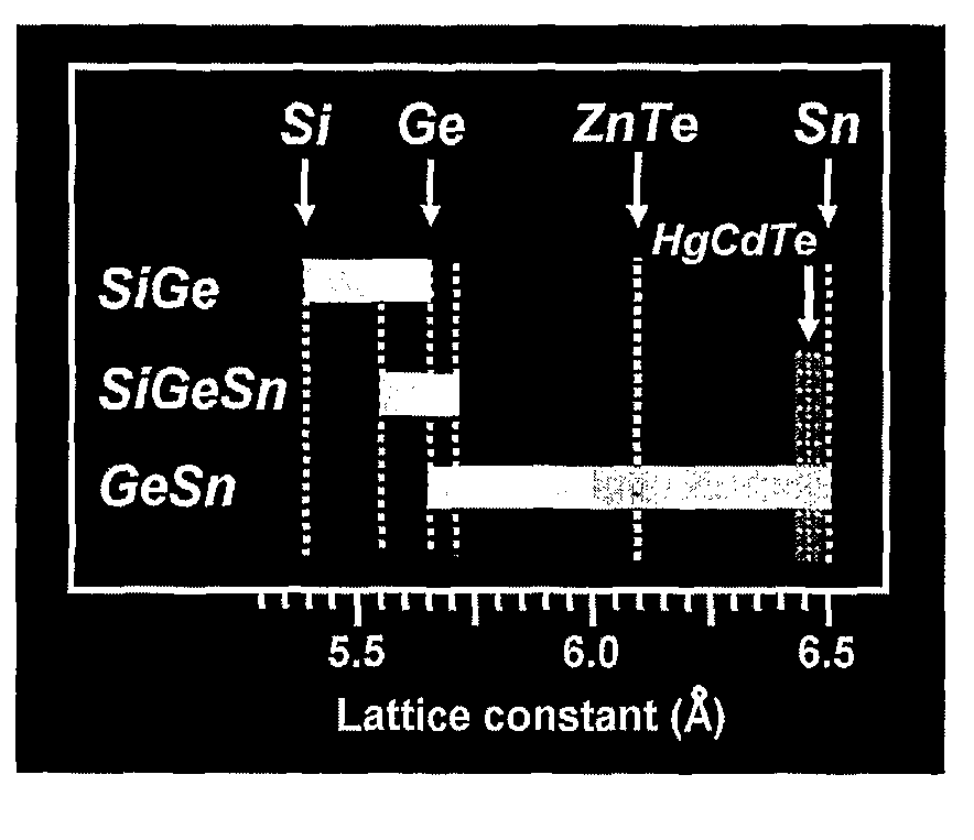
Although Si and Ge are closely related, direct epitaxy of Ge on Si produces copious defects in the Ge layer due to a significant lattice and thermal mismatch.
While the above approach is relatively straightforward it poses several limitations: (1) the addressable lattice parameter space is limited to a narrow range between Si and Ge, thus allowing lattice matching of only three compounds (GaAs, GaP, and AIP); (2) the process requires thick buffer layers grown at a relatively high temperature, which causes additional defect formation due to thermal mismatch; (3) a post-growth, CMP planarization step is mandatory; and (4) threading defect densities are in the 106 per cm2 range, which is detrimental to most advanced compound devices; a reduction in defect density of two to three orders of magnitude is needed.

Method used


Image

  • GeSiSn-based compounds, templates, and semiconductor structures
  • GeSiSn-based compounds, templates, and semiconductor structures
  • GeSiSn-based compounds, templates, and semiconductor structures

Examples


example 1

GeSn Surface Preparation And Examples of Si Integration

[0111]The GeSn buffer layer surface can be prepared by extremely simple chemical cleaning methods for subsequent ex-situ epitaxial growth. This is an essential enabling step that further demonstrates the feasibility of these materials as versatile templates for integration with Si. GeSn films with the desired thickness and Sn concentration are grown on Si substrates with a nominal size of 2.5×3.0 cm2. A single typical deposition experiment produces a batch of 4-10 wafers. We routinely characterize several randomly selected samples from each batch using RBS (Rutherford backscattering spectroscopy), atomic force microscopy (AFM) and x-ray diffraction to evaluate the quality of the films. RBS ion channeling is used to gauge qualitative the presence of threading dislocations that propagate across the layer thickness. In most samples, the ratio of the aligned versus the random peak heights (χmin), which measures the degree of crystal...

example 2

Examples Of Growth Of III-V Materials On Si Via Si—Ge—Sn Buffer Layers: GaAs, AlGaAs, GaAsSb and InGaAs

[0113]As a demonstration of the applicability of the GeSn film as buffer layers for integration of semiconductors with Si we explored direct growth of III-V compounds on GeSn / Si substrates. We grew pure GaAs (a=5.65 Å) layers as well as AlGaAs / GaAs quantum well structures on nearly lattice-matched GeSn (a=5.67 Å) buffer layers. For comparison we simultaneously conducted growth of the same materials on GaAs substrates via homoepitaxy. In both cases we have determined the structural, morphological and optical properties of the films by XTEM, AFM, photoluminescence (PL), and high resolution XRD. We find that the quality of the films grown on GaAs substrates (including PL peak positions) is comparable to that grown on GeSn / Si buffer layers indicating that our methodology in this case works and our approach may offer a convenient and low cost route to the integration of compound semicon...

example 3

References for Example 3

[0155][1] Resonant cavity enhanced InGaAs photodiodes for high speed detection of 1.55 μm infrared radiation, Kaniewski J., Muszalski J., Pawluczyk J., Piotrowski J., Proceedings of SPIE-The International Society for Optical Engineering (2005), 5783 (Pt. 1, Infrared Technology and Applications XXXI), 47-56.[0156][2] InGaAs-on-Si single photon avalanche photodetectors, Kang Y., Lo Y.-H., Bitter M., Kristjansson S., Pan Z., Pauchard A., Applied Physics Letters (2004), 85(10), 1668-1670.[0157][3] High Performance 0.1 μm GaAs Pseudomorphic High Electron Mobility Transistors with Si Pulse-Doped Cap Layer for 77 GHz Car Radar Applications, Kim S., Noh H., Jang K., Lee J., Seo K., Jpn. J. App. Phys. 44, 2472-2475 (2005).[0158][4] Growth of AlAsSb / InGaAs MBE-layers for all-optical switches, Cristea P., Fedoryshyn Y., Jaeckel H., J. Cryst. Growth 278(1-4), 544-547 (2005).[0159][5] Improved characteristics of metamorphic InAlAs / InGaAs high electron mobility transistor ...


PUM

PropertyMeasurementUnit
thicknessaaaaaaaaaa
thicknessaaaaaaaaaa
boiling pointaaaaaaaaaa

Abstract

The present invention provides novel compounds of the formula Gei-x-ySixSny, wherein 0.01<y<0.11, and 0.26<x<0.35, and semiconductor structures comprising such compounds. The present invention also provides novel semiconductor structures comprising silicon substrates, an SiGe buffer layer, and a Group III-V or II-VI active layer. The present invention also provides novel semiconductor structures comprising silicon substrates, an SiGe buffer layer, an SiGeSn template layer, and an SiGe, Ge, Group III-V, or Group II-VI active layer.

Description

CROSS REFERENCE[0001]This application claims priority to U.S. Provisional Patent Application Ser. No. 60 / 660,779, filed Mar. 11, 2005, which is incorporated by reference herein in its entirety.STATEMENT OF GOVERNMENT FUNDING[0002]Financial assistance for this invention was provided by the United States Government, National Science Foundation Grant Number DMR 0221993 and Air Force Office for Scientific Research under Contract AFRL / SNHC (F19628-03-C-0056). Therefore, the United States Government may own certain rights to this invention.FIELD OF THE INVENTION[0003]This invention relates generally to GeSiSn-based compounds, templates, and semiconductor structures derived therefrom.BACKGROUND OF THE INVENTION[0004]The concept of buffer layers is well-known and widely used in heteroepitaxy of semiconductors. They are designed to alleviate interfacial stress and defect formation or to promote growth of certain phases or 2D morphology. For highly mismatched systems, the concept of graded bu...

Claims


Application Information

Patent Timeline
Patent Type & Authority Patents(United States)
IPC IPC(8): B32B15/04C01B33/00
CPCC23C16/0272C23C16/301C23C16/42C30B25/02C30B29/52H01L21/02381H01L21/0245H01L21/02452H01L21/02502H01L21/02532H01L21/02535H01L21/02543H01L21/02546H01L21/02549H01L21/02557H01L21/0256H01L21/02562H01L21/02568H01L21/0262H01L29/161H01L29/165H01L29/267H01L31/028H01L31/0296H01L31/0304H01L31/03046H01L31/101H01L29/20H01L29/22Y02E10/544Y02E10/547C01G17/00
Inventor KOUVETAKIS, JOHNROUCKA, RADEK
Owner ARIZONA STATE UNIVERSITY
Learn More