
Thermally enhanced semiconductor package

a technology of semiconductors and packaging, applied in the direction of semiconductor devices, semiconductor/solid-state device details, semiconductor devices, etc., can solve the problems of increasing the thermal stress on the chip, reducing the reliability reducing the thermal performance of the integrated circuit, so as to improve the thermal package structure and methods.

Inactive Publication Date: 2011-09-13
MAXIM INTEGRATED PROD INC
View PDF9 Cites 9 Cited by
  • Summary
  • Abstract
  • Description
  • Claims
  • Application Information

AI Technical Summary

Benefits of technology

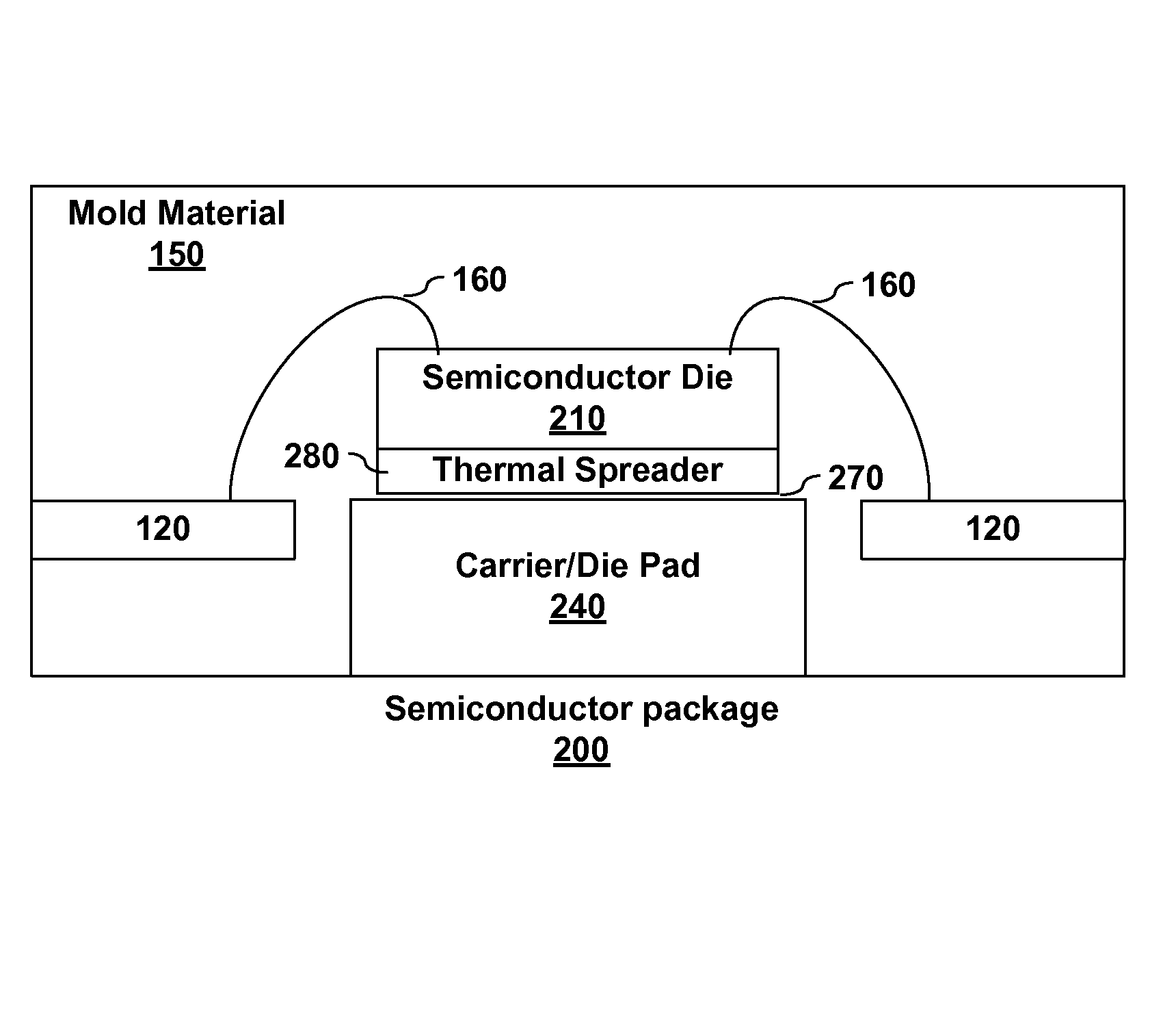
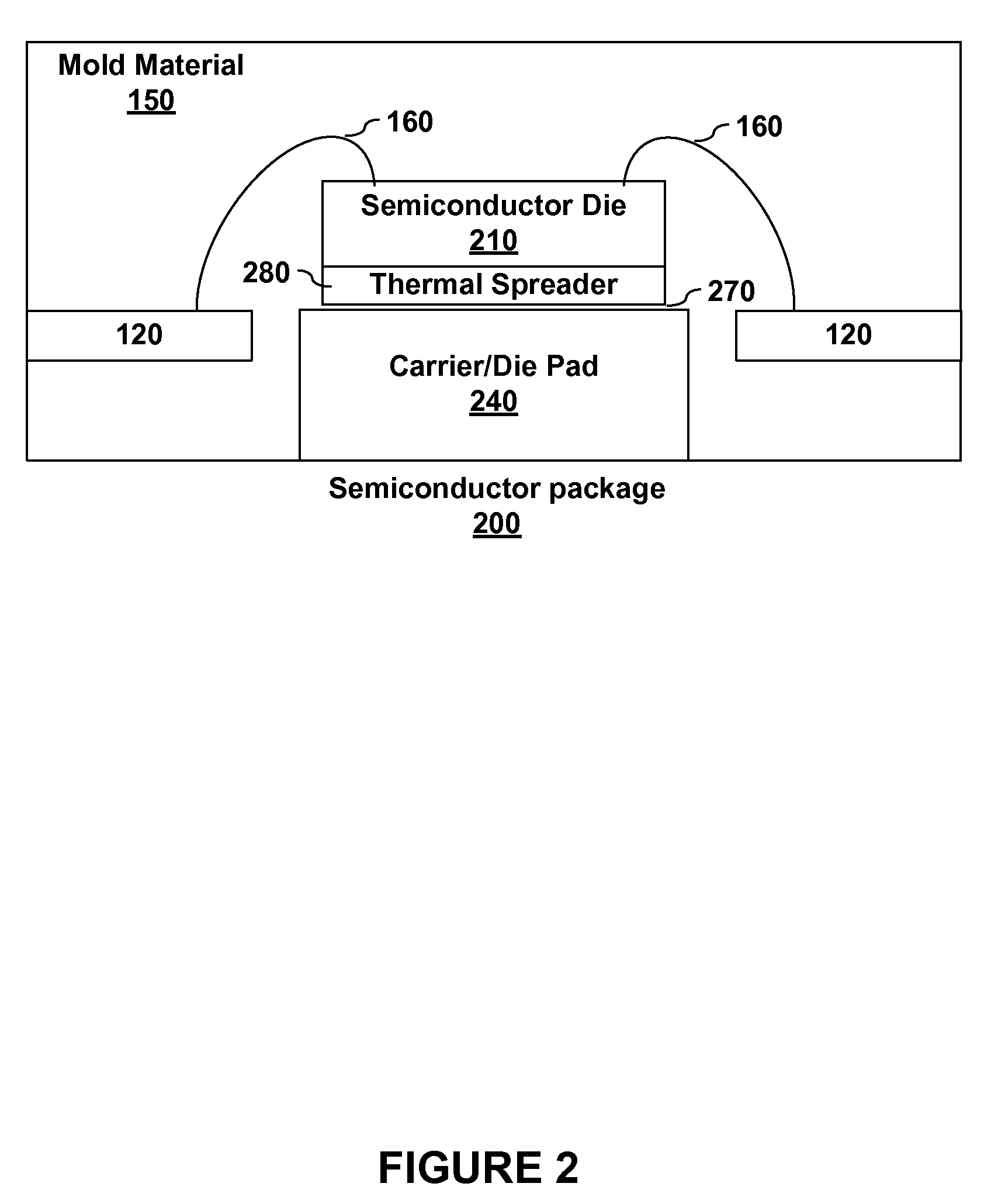
[0007]Given the above drawbacks, an objective of the present invention is to provide improved thermal package structures and methods for manufacturing the same, through the application of one or more thermal spreaders embedded inside the package. In embodiments, a thermal spreader is incorporated in a semiconductor package between a semiconductor die and its support, which may also be referred to herein as a carrier, a substrate, or a die pad. In embodiments, the die thickness may be suitably reduced so that the overall package thickness remains unchanged relative to corresponding conventional packages. Higher levels of heat spreading accomplished through integration of the thermal spreader help the chip function at cooler temperatures.
[0008]Another object of the present invention is to provide die shrink possibilities and possibilities of enhancing package level integration. Because the thermally enhanced package is able to handle higher power densities, the die may be shrunk and still operated within thermal limits. In embodiments, one or more of the specifications of a thermally enhanced semiconductor package can remain constant relative to a non-thermally enhanced semiconductor package (such as package dimension and function), thereby sparing a customer of the chip package from any major changes to its application board or manufacturing process.
[0009]Yet another object of the present invention is to facilitate possibilities of smaller package footprints than that of the conventional packages. In embodiments, the improved thermal performance created by the introduction of one or more thermal spreaders allows for the reduction of die size, semiconductor packages with a smaller footprint but the same or improved performance can be produced. By leveraging a die size reduction through an advanced silicon (or other semiconductor) technology as well as leveraging the package thermal enhancements through the use of an integrated thermal spreader, a chip developer can provide semiconductor packages with the same or improved performance but with a smaller form factor. As products move toward smaller form factors, being able to produce chips with smaller sizes can provide the end user with significant space savings at a system- or sub-system level.

Problems solved by technology

Integrated circuits, also referred to chips, microchips, or semiconductor dies, are fragile and susceptible to many factors, such as mechanical stresses, chemical stresses, and thermal stresses.
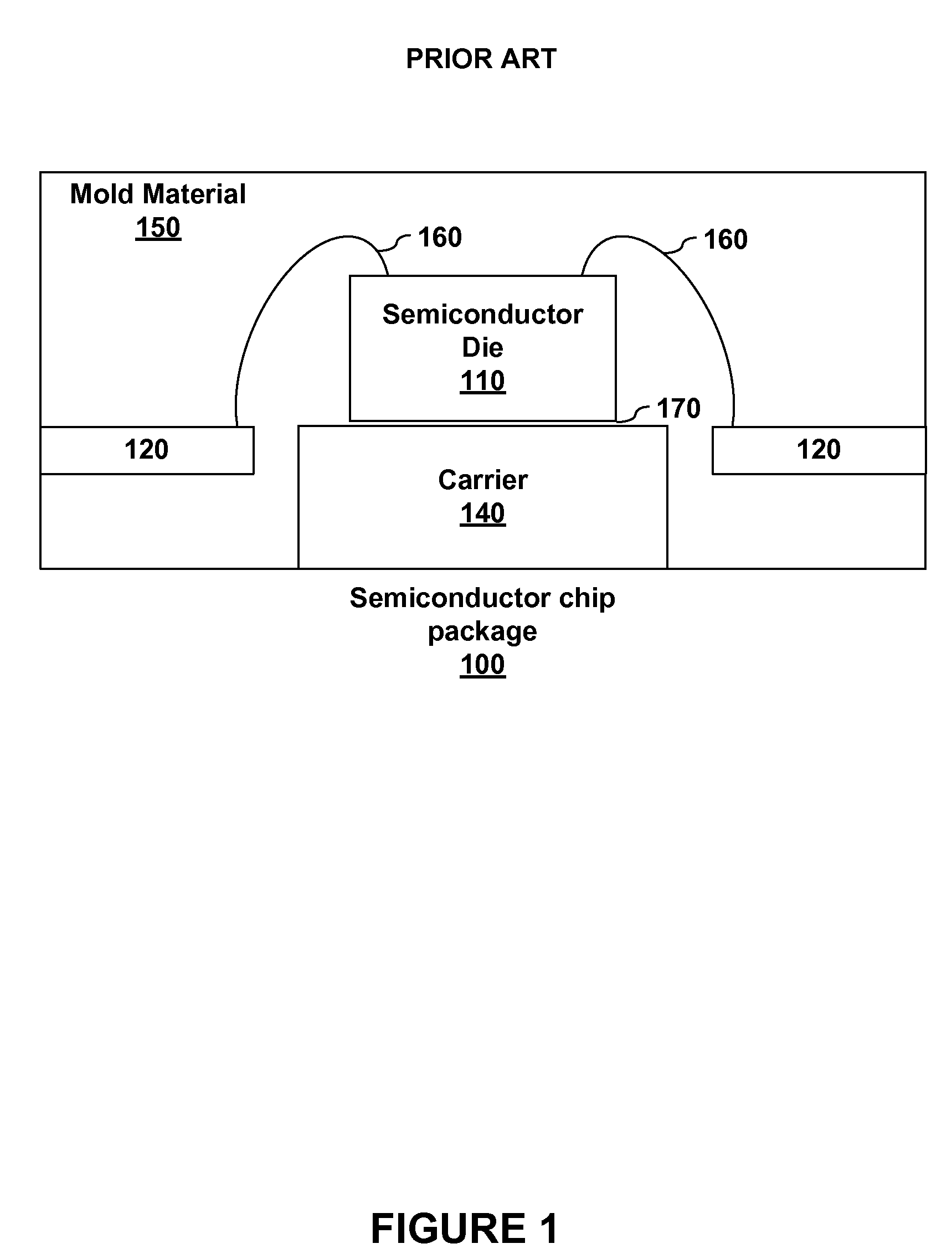
However, the addition of material around the integrated circuit from the packaging can increase the thermal resistance and thereby increase thermal stresses on the chip.
These thermal stresses can reduce the reliability of the integrated circuit and, in some cases, can result in its catastrophic failure.
When inside a package, the thermal resistance created by the packaging can inhibit the chip's ability to dissipate this generated heat.
The thermal issues become more acute with increasing levels of power dissipation.
These thermal issues amplify the possibilities of decreased chip performance and failure due to excess heat.

Method used


Image

  • Thermally enhanced semiconductor package
  • Thermally enhanced semiconductor package
  • Thermally enhanced semiconductor package

Examples


Embodiment Construction

[0028]In the following description, for purpose of explanation, specific details are set forth in order to provide an understanding of the invention. It will be apparent, however, to one skilled in the art that the invention may be practiced without these details. One skilled in the art will recognize that embodiments of the present invention, some of which are described below, may be incorporated into a number of different systems and devices.

[0029]Components shown in block diagrams are illustrative of exemplary embodiments of the invention and are meant to avoid obscuring the invention. It shall also be understood that throughout this discussion that components may be described as separate units, which may comprise sub-units, but those skilled in the art will recognize that, in embodiments, the various components, or portions thereof, may be divided into separate components or may be integrated together.

[0030]Furthermore, connections between components within the figures are not i...


PUM


Abstract

Disclosed are systems and methods for improving the thermal performance of integrated circuit packages. Aspects of the present invention include improved thermal package structures and methods for producing the same through the application of one or more thermal spreaders in the package. In embodiments, a thermal spreader is incorporated in a semiconductor chip package between a semiconductor die and its die pad. By including a thermal spreader in an IC package, the package can handle higher levels of power while maintaining approximately the same temperature of the package or can reduce the temperature of the package when operating at the same power level, as compared to a package without a thermal spreader.

Description

BACKGROUND[0001]A. Technical Field[0002]The present invention relates generally to systems and methods for integrated circuit (“IC”) packaging. And, the present invention relates more particularly to systems and methods for improving the thermal performance of integrated circuit package solutions.[0003]B. Background of the Invention[0004]Integrated circuits, also referred to chips, microchips, or semiconductor dies, are fragile and susceptible to many factors, such as mechanical stresses, chemical stresses, and thermal stresses. Prior to being used in an electronic system, an integrated circuit must be packaged to help minimize the impact of these stress factors. Packaging helps protect against mechanical stresses by providing structural support to the integrated circuit. By encapsulating the integrated circuit in a package, the integrated circuit is protected against environmental factors such as dust, moisture, and other items that could cause chemical stress or otherwise affect t...

Claims


Application Information

Patent Timeline
Patent Type & Authority Patents(United States)
IPC IPC(8): H01L23/10H01L23/495
CPCH01L23/4334H01L23/49568H01L24/32H01L23/49575H01L2924/01019H01L2924/01006H01L24/48H01L2924/14H01L2924/01082H01L2924/01079H01L2924/01078H01L2924/01074H01L2224/32145H01L2224/32245H01L2224/48091H01L2224/48247H01L2224/73265H01L2924/01005H01L2924/01029H01L2924/01033H01L2924/01047H01L2924/00014H01L2924/00012H01L24/73H01L2924/181H01L2924/351H01L2924/00H01L2224/45099H01L2224/45015H01L2924/207
Inventor RAILKAR, TARAK A.CATE, STEVEN D.
Owner MAXIM INTEGRATED PROD INC
Learn More