
Multi-chip package structure and method of fabricating the same

a multi-chip and package technology, applied in the direction of semiconductor devices, semiconductor/solid-state device details, electrical devices, etc., can solve the problems of deteriorating the competitiveness of relevant products, and achieve the effect of reducing the thickness and dimension of the entire multi-chip package structure and simplifying the circuit layout of the carrier

Active Publication Date: 2011-06-28
ADVANCED SEMICON ENG INC
View PDF6 Cites 2 Cited by
  • Summary
  • Abstract
  • Description
  • Claims
  • Application Information

AI Technical Summary

Benefits of technology

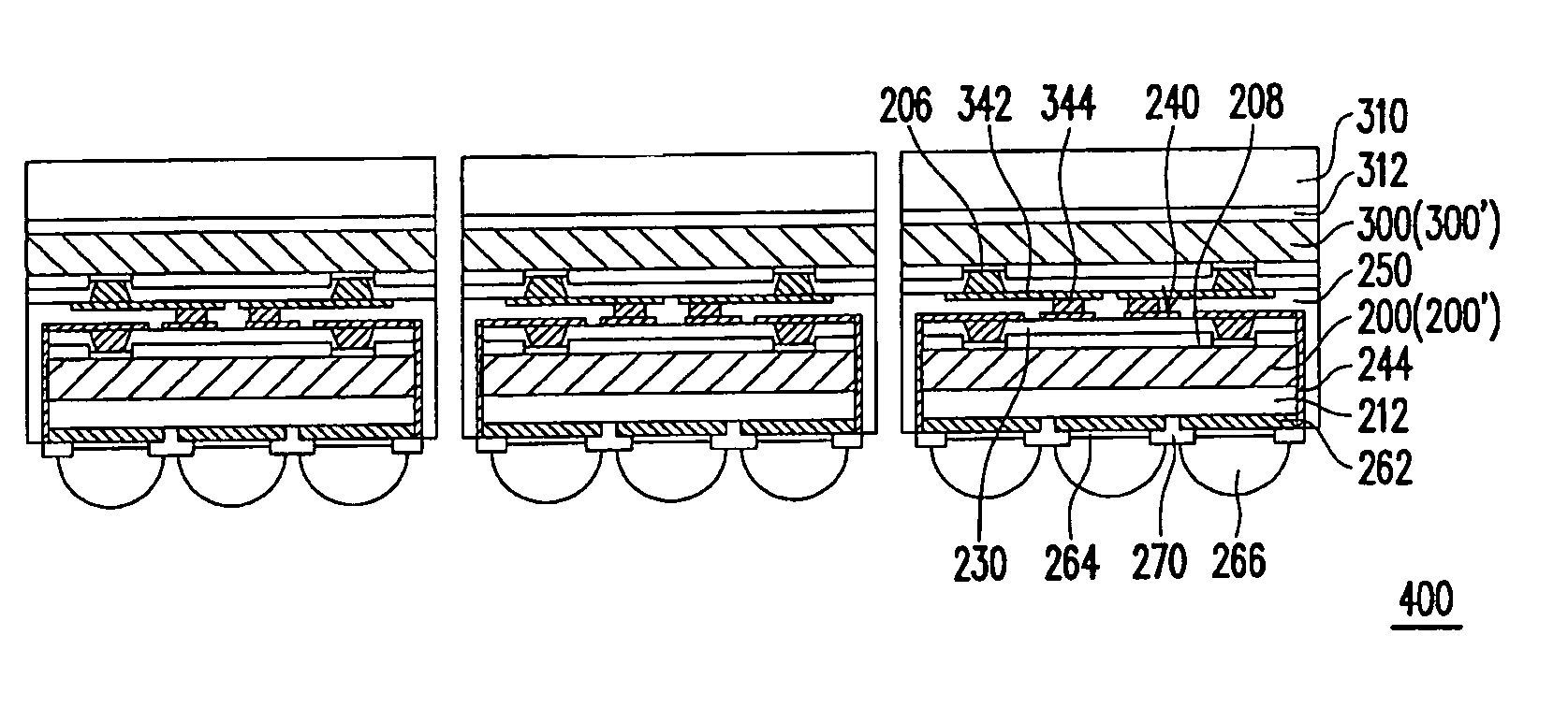
The present invention provides a method of fabricating a multi-chip package structure that reduces the thickness and dimension of the package, simplifies the circuit layout of the carrier, and enhances insulating properties. The method includes forming conductive walls on a first chip, adhering a first metal layer to the chip, patterning the metal layer to expose pads, and then adhering a substrate to the metal layer. The method also includes forming a cover layer on the chip, exposing the pads, and connecting the pads to a second chip using conductive bumps. The multi-chip package structure includes a first circuit layer and a second circuit layer, and the conductive walls connect the two layers. The method and structure provide improved performance and reliability for multi-chip package structures.

Problems solved by technology

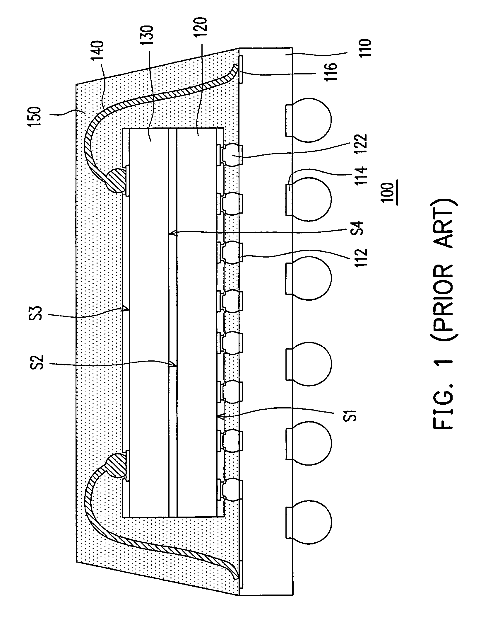
However, the entire thickness and the dimension of the multi-chip package structure 100 are not apt to be reduced, thus diverging from the demands on miniaturization of the chip package structures and deteriorating the competitiveness of relevant products.

Method used


Image

  • Multi-chip package structure and method of fabricating the same
  • Multi-chip package structure and method of fabricating the same
  • Multi-chip package structure and method of fabricating the same

Examples


Embodiment Construction

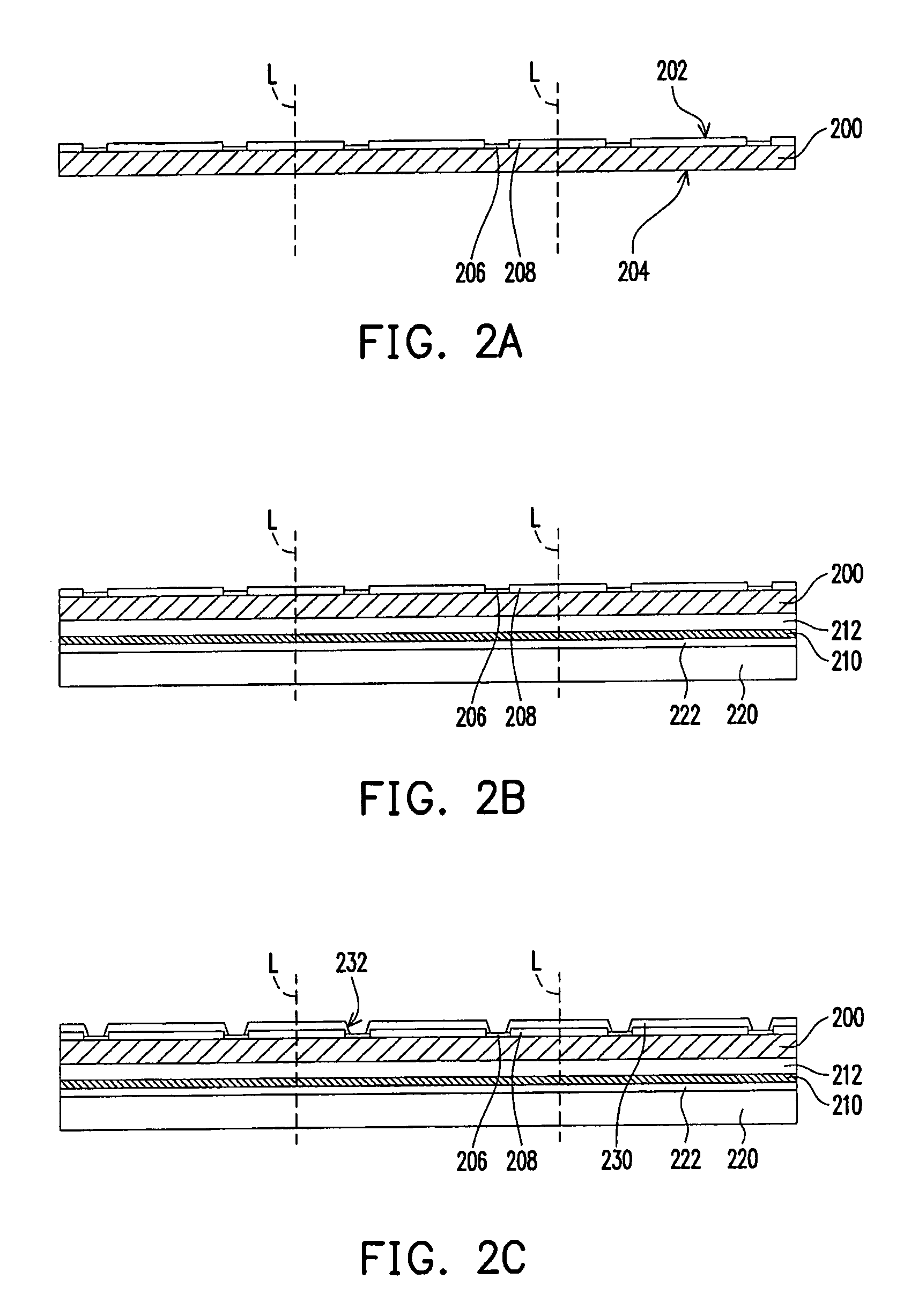
[0029]FIGS. 2A through 2G are schematic views illustrating a front-end stage of a method of fabricating a multi-chip package structure according to an embodiment of the present invention. Steps of the method of fabricating the multi-chip package structure in the front-end stage are mainly performed on a first wafer 200. Please refer to the embodiment illustrated in FIGS. 2A and 2B. First, the first wafer 200 is provided, on which the IC layout and the IC fabrication are completed. The first wafer 200 includes an active surface 202 and a back surface 204 opposite thereto. A plurality of bonding pads 206 is disposed on the active surface 202 and exposed by a passivation layer 208 covering the active surface 202. In a second step, a first metal layer 210 and a substrate 220 are adhered to the back surface 204 of the first wafer 200. The first metal layer 210 is interposed between the first wafer 200 and the substrate 220. The first metal layer 210 is adhered to the back surface 204 of ...


PUM


Abstract

A method of fabricating a multi-chip package structure is provided. In the method, a number of cavities are formed on a predetermined cutting line of a first wafer by partly removing the first wafer and a first metal layer. Conductive walls of a first circuit layer are electrically connected to a cut cross-section of the first metal layer exposed by the cavities. In addition, conductive bumps of a second wafer are pressed into a cover layer and electrically connected to the first circuit layer. The first metal layer is then patterned to form a second circuit layer having a number of second pads. Next, the first wafer and the second wafer are cut along the predetermined cutting line to form a number of separated multi-chip package structures.

Description

CROSS-REFERENCE TO RELATED APPLICATION[0001]This application claims the priority benefit of Taiwan application serial no. 97107328, filed on Mar. 3, 2008. The entirety of the above-mentioned patent application is hereby incorporated by reference herein and made a part of this specification.BACKGROUND OF THE INVENTION[0002]1. Field of the Invention[0003]The present invention relates to a semiconductor package process. More particularly, the present invention relates to a method of fabricating a multi-chip package structure.[0004]2. Description of Related Art[0005]With an advancement of semiconductor technologies, high density integrated circuit (IC) packages such as ball grid array (BGA) packages, chip-scale packages (CSPs), flip chip (F / C) packages, and multi-chip module (MCM) packages have been correspondingly developed. On account of an application of bumps instead of wires for reducing the length of connection circuits between chips and carriers in the above-mentioned high densit...

Claims


Application Information

Patent Timeline
Patent Type & Authority Patents(United States)
IPC IPC(8): H01L23/02
CPCH01L21/6835H01L21/6836H01L25/50H01L21/561H01L2225/06513H01L2224/73265H01L2224/48465H01L2224/48091H01L23/3114H01L2221/68327H01L2221/68372H01L2224/16225H01L2924/00014H01L2924/00H01L2924/181H01L2224/32145H01L2924/00012
Inventor WANG, CHIEN-HAO
Owner ADVANCED SEMICON ENG INC
Learn More