
Methods, materials and devices for light manipulation with oriented molecular assemblies in micronscale photonic circuit elements with High-Q or slow light

a technology of photonic circuit elements and molecular assemblies, which is applied in the direction of optical elements, instruments, vacuum evaporation coatings, etc., can solve the problems of thermal irreversibility, high fatigue resistance, and high speed of molecular self-assemblies for direct modulation (control) of light propagation in photonic microstructures, and achieve enhanced interaction with single molecules, molecular layers or aggregates.

Inactive Publication Date: 2011-06-07
PRESIDENT & FELLOWS OF HARVARD COLLEGE
View PDF30 Cites 20 Cited by
  • Summary
  • Abstract
  • Description
  • Claims
  • Application Information

AI Technical Summary

Benefits of technology

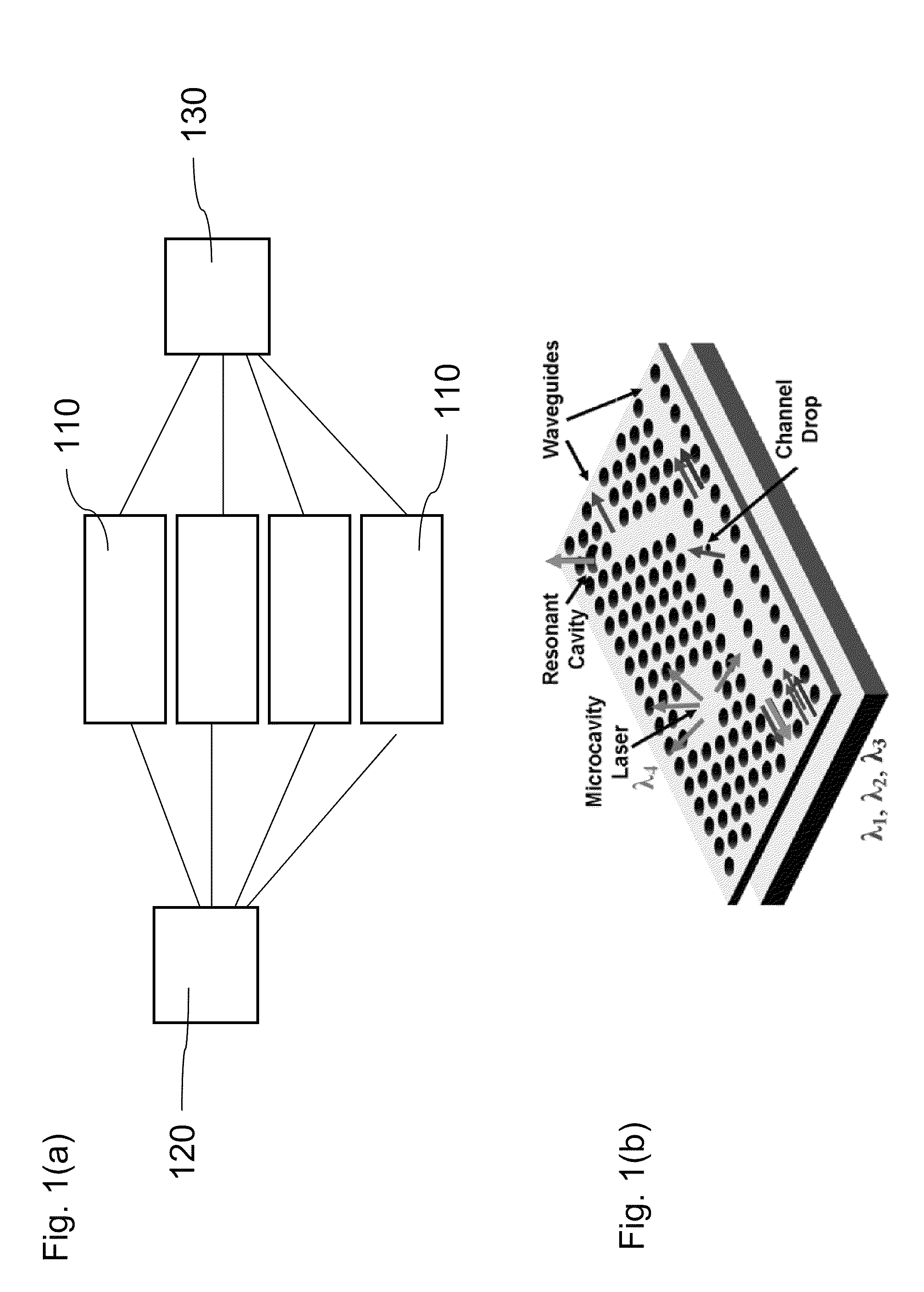
The present invention is about creating hybrid molecular-photonic circuits (MPCs) that use ordered molecules and nanostructures for optical manipulation on a small scale. The invention makes use of photonic circuit elements that enhance the interaction with a single molecule, allowing for the performance of basic photonic functions such as logic operations, memory, and tunable wavelength division multiplexing. The MPCs can be used as all-optical switches and routers, and can manipulate intense IR light with low intensity visible control pumps. The invention also includes an optical device that includes an input waveguide, output waveguide, and a high-Q resonant or photonic structure that generates slow light connected to the input and output waveguides. The MPCs can be made from a variety of materials, including organic or biological molecules, molecular layers, or nanostructures. The technical effects of the invention include enhanced optical manipulation on a small scale, improved sensitivity to molecular dynamics, and increased control over molecular polarizabilities.

Problems solved by technology

The expected weak optical response of a single molecular layer, however, has prevented the use of molecular self-assemblies for the direct modulation (control) of light propagation in photonic microstructures.
Such applications generally require high speed, thermal irreversibility and high-fatigue resistance.

Method used


Image

  • Methods, materials and devices for light manipulation with oriented molecular assemblies in micronscale photonic circuit elements with High-Q or slow light
  • Methods, materials and devices for light manipulation with oriented molecular assemblies in micronscale photonic circuit elements with High-Q or slow light
  • Methods, materials and devices for light manipulation with oriented molecular assemblies in micronscale photonic circuit elements with High-Q or slow light

Examples


Embodiment Construction

[0072]All-optical switches and logic gates are needed as components in integrated photonic circuits that control the flow of light at near-infrared (IR) frequencies. The recent drive to optical device miniaturization exemplified by the emergence of photonic bandgap nanostructures suggests molecules as possible functional elements. However, materials with a strong optical response in the near-IR, necessary for direct modulation at small scales, are generally unavailable. This limitation may be overcome by resonant amplification of the otherwise weak optical response through light recirculation in optical (high-Q) cavities or in photonic structures that generate slow light. High-Q cavities and slow light devices can be micro-fabricated. Common photonic architectures are ring resonators or photonic crystals—which also provide a convenient platform to interface with molecular aggregates. Molecules can be crafted on the surface or directly into the optical path of the photonic structure ...


PUM

PropertyMeasurementUnit
absorption wavelengthsaaaaaaaaaa
absorption wavelengthaaaaaaaaaa

Abstract

An optical device that comprises an input waveguide, an output waveguide, a high-Q resonant or photonic structure that generate slow light connected to the input waveguide and the output waveguide, and an interface, surface or mode volume modified with at least one material formed from a single molecule, an ordered aggregate of molecules or nanostructures. The optical device may include more than one input waveguide, output waveguide, high-Q resonant or photonic structure and interface, surface or mode volume. The high-Q resonant or photonic structure may comprise at least one selected from the group of: microspherical cavities, microtoroidal cavities, microring-cavities, photonic crystal defect cavities, fabry-perot cavities, photonic crystal waveguides. The ordered aggregate of molecules or nanostructures comprises at least one selected from the group of: organic or biological monolayers, biological complexes, cell membranes, bacterial membranes, virus assemblies, nanowire or nanotube assemblies, quantum-dot assemblies, one or more assemblies containing one or more rhodopsins, green fluorescence proteins, diarylethers, lipid bilayers, chloroplasts or components, mitochondria or components, cellular or bacterial organelles or components, bacterial S-layers, photochromic molecules. Further, the molecular aggregate may exhibit a photoinduced response.

Description

CROSS-REFERENCE TO RELATED APPLICATIONS[0001]The present application claims the benefit of the filing date of U.S. Provisional Patent Application Ser. No. 60 / 747,041 entitled “Methods, Materials And Devices For Light Manipulation With Oriented Molecular Assemblies In Micronscale Photonic Circuit Elements With High-Q Or Slow Light” and filed on May 11, 2006 by inventors Frank Vollmer and Juraj Topolancik.[0002]Also, related subject matter is disclosed in U.S. Provisional Patent Application Ser. No. 60 / 758,040 entitled “Optical Device and Method for Detection using Optical Cavities such as Ring Resonators or Microsphere, -Disk, -Ring or -Toroid Cavities that contain a Gain Medium such as Erbium” and filed by Frank Vollmer on Jan. 11, 2006.[0003]The above cross-referenced related applications are hereby incorporated by reference herein in its entirety.STATEMENT REGARDING FEDERALLY SPONSORED RESEARCH OR DEVELOPMENT[0004]None.BACKGROUND OF THE INVENTION[0005]1. Field of the Invention[000...

Claims


Application Information

Patent Timeline
Patent Type & Authority Patents(United States)
IPC IPC(8): G02B6/26
CPCB82Y20/00G02B6/1225G02F1/0126G02F1/3511G02F2202/32G02F2203/15
Inventor VOLLMER, FRANKTOPOLANCIK, JURAJ
Owner PRESIDENT & FELLOWS OF HARVARD COLLEGE
Learn More