
IC tag

a technology of ic tags and resonant antennas, applied in the field of noncontact ic tags, can solve the problems of low reliability of ic tags produced, damage to electrical circuits in formation of broken lines, etc., and achieve the effect of reliably deactivating ic tags and visual confirmation of deactivation

Inactive Publication Date: 2011-05-31
LINTEC CORP
View PDF8 Cites 0 Cited by
  • Summary
  • Abstract
  • Description
  • Claims
  • Application Information

AI Technical Summary

Benefits of technology

The present invention aims to provide an IC tag that can be produced by a simplified process, can be reliably deactivated in the use, and can be deactivated without using any special apparatus. The invention achieves this by forming a terminal for formation of broken line in the wiring of electronic circuit, and a broken line that penetrates through the substrate and the surface circuit. The invention also includes a surface protective layer and an adhesive layer for deactivation. The invention allows the step of formation of broken line to be contained in the step of cutting a size of tags into individual tags, and the deactivation of IC tag can be confirmed visually. The invention also reduces the risk of low processing accuracy in the formation of broken line, resulting in improved reliability of the IC tag.

Problems solved by technology

With this IC tag, however, there is a risk that, when the processing accuracy in the process of IC tag production is low, the electronic circuit is destroyed in formation of broken line.
In such a case, the IC tag produced has low reliability.

Method used


Image

  • IC tag
  • IC tag
  • IC tag

Examples


example 1

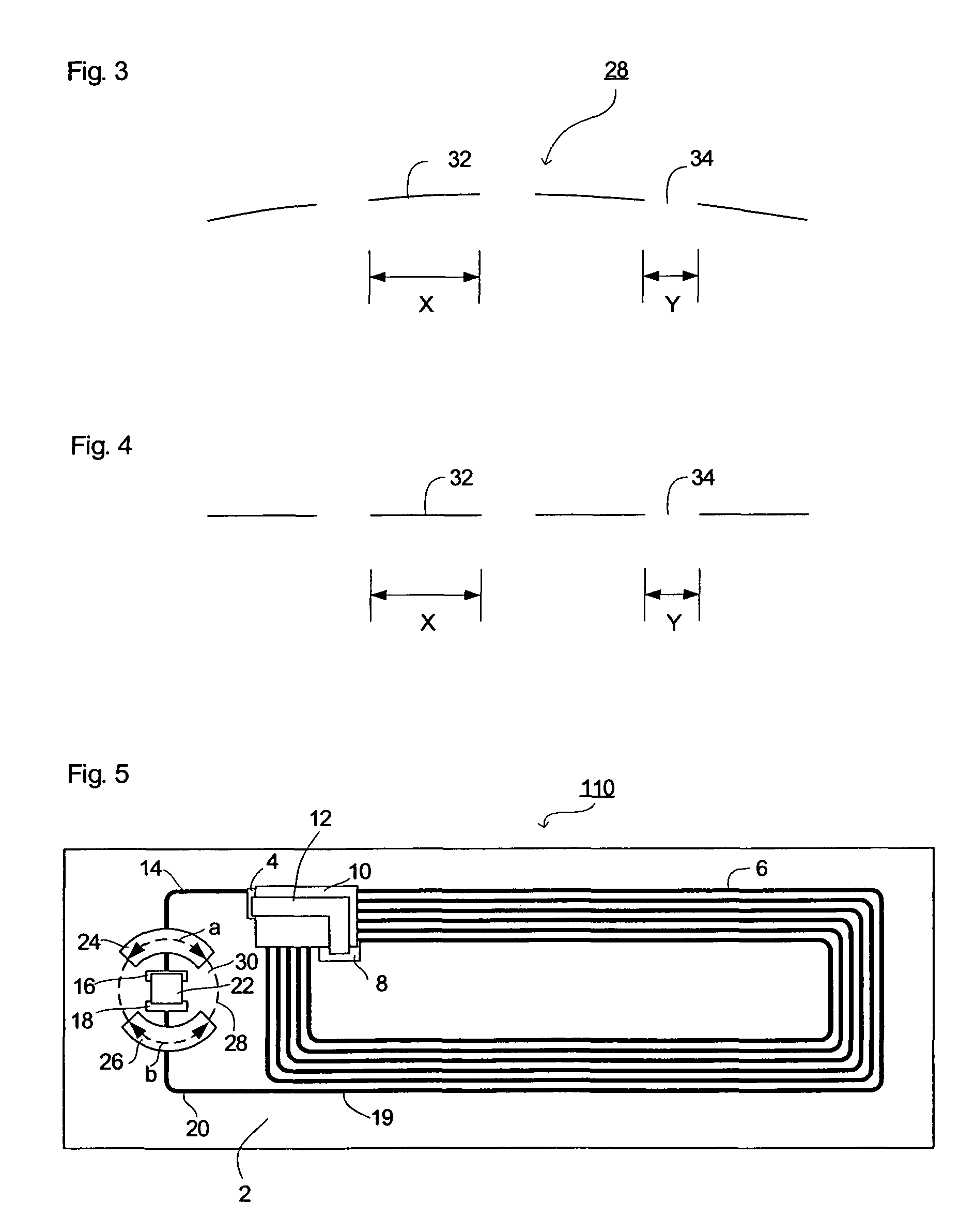
[0114]An IC inlet shown in FIG. 5 was produced and, using the IC inlet, an IC tag shown in FIG. 7 was produced by a procedure described below.

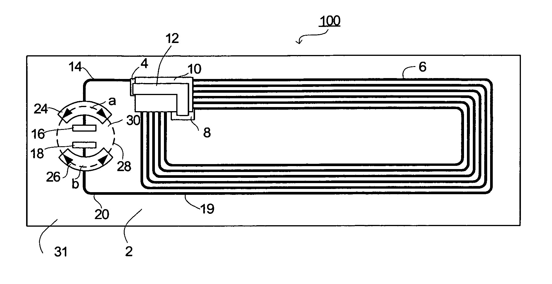
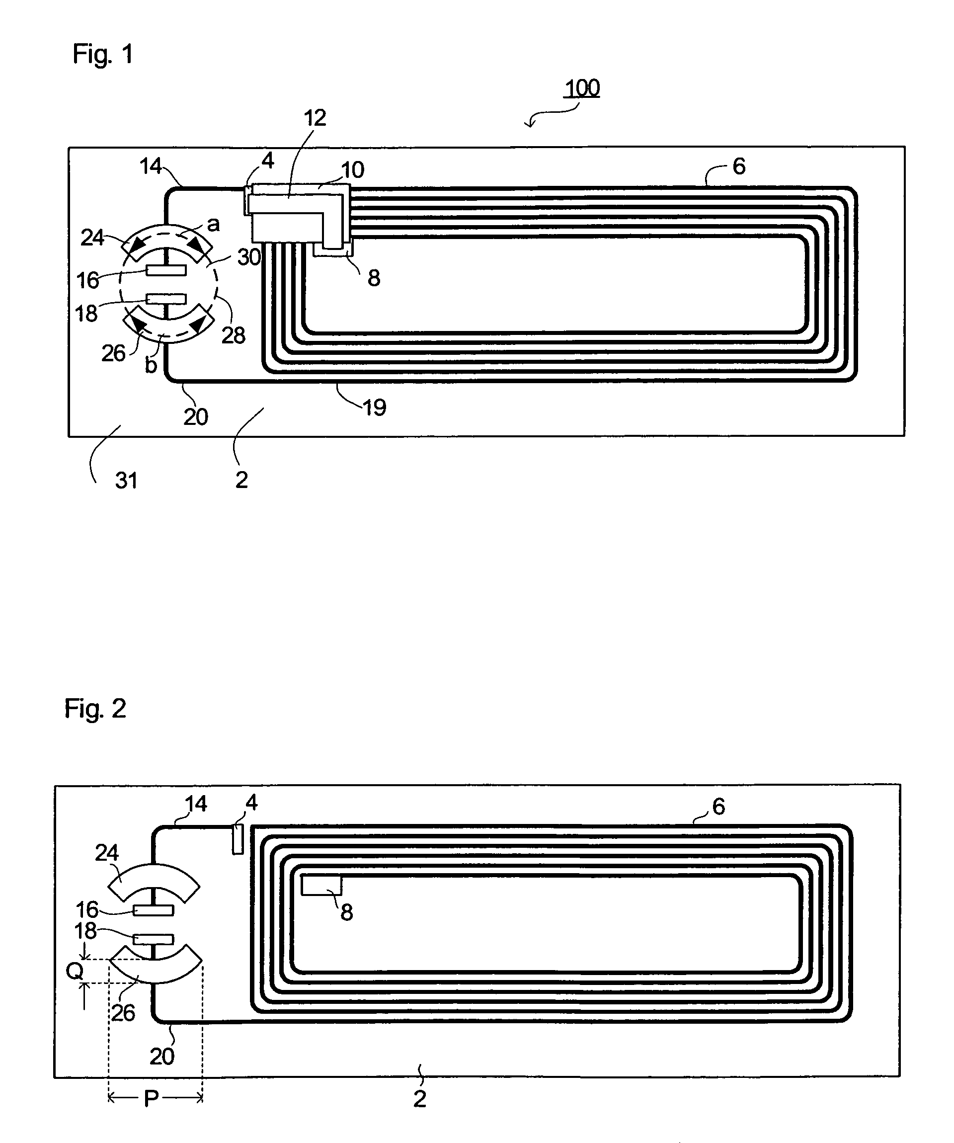
[0115]First, there was prepared a composite sheet [NIKAFLEX (trade name) produced by NIKKAN INDUSTRIES Co., Ltd., Cu / PET=35 μm / 50 μm] which is made by laminating a copper foil and a polyethylene terephthalate film (PET). On this sheet was printed, by screen printing, a resist pattern for formation of outer taking-out electrode 4, planar coil circuit portion 6, inner taking-out electrode 8, opposed electrodes 16 and 18, leads 14 and 20 and terminals for formation of broken line 24 and 26. The resulting sheet was subjected to etching to remove unnecessary copper foil portions, whereby a unified wiring pattern shown in FIG. 2 was produced.

[0116]The line width of the circuit was 0.2 mm.

[0117]Then, between the outer taking-out electrode 4 and the inner taking-out electrode 8, an insulating layer 10 was formed so as to cover the planar coil circuit ...

example 2

[0125]20 pieces of IC tags were produced in the same manner as in Example 1 except that terminals for formation of broken line 24 and 26 were formed using a silver paste. The terminals for formation of broken line 24 and 26, formed with a silver paste were formed by screen printing, simultaneously with the formation of a jumper 12. An IC chip was mounted and each resulting IC tag was confirmed for RFID function in the same manner as in Example 1. Then, the IC tag was attached to a polypropylene resin plate. 24 hours later, the IC tag was peeled from the resin plate. As a result, the IC tags of 20 pieces were cut off along the broken line, the circuit of each IC tag was destroyed physically, and the RFID function was lost.

example 3

[0126]20 pieces of IC tags were produced in the same manner as in Example 1. However, as shown in FIG. 6, a rectangular terminal for formation of broken line 62 of 10 mm in length and 15 mm in width was formed in a lead 20, and a closed rectangular broken line 64 of 15 mm in length and 5 mm in width was formed so as to divide the terminal for formation of broken line 62 into two parts. Each side of the rectangular broken line 64 was consisted of four straight lines as shown in FIG. 4; and the length Y of each uncut part 34: the length X of each cut part 32=1:2, and the length Y of each uncut part was 0.5 mm.

[0127]In the same manner as in Example 1, there was laminated a release material coated, by a screen coater, with an acrylic adhesive at the release treatment-applied side, on the whole portion of the substrate 2 side on which a circuit was formed.

[0128]Each resulting IC tag was confirmed for RFID function. Then, the IC tag was attached to a polypropylene resin plate. 24 hours la...


PUM


Abstract

According to the present invention, there is disclosed an antenna circuit characterized by comprising:a substrate,a surface circuit consisting of a planar coil circuit portion and at least one pair of opposed electrodes connected to the planar coil circuit portion formed on the substrate,at least one terminal for formation of broken line, formed in a conductor constituting the surface circuit, and a broken line which penetrates through the substrate and the surface circuit and which has, in the terminal for formation of broken line, at least one uncut part passing through the terminal for formation of broken line.

Description

TECHNICAL FIELD[0001]The present invention relates to a non-contact IC tag used in confirmation of individuals, merchandise management, physical distribution management, etc.BACKGROUND ART[0002]In recent years, there has been widely used non-contact IC tag which is attached to-be-controlled persons or goods (adherends) for control of the flow, circulation, etc. of such persons or goods. This IC tag can memorize data in the IC chip built therein. By allowing the IC tag to communicate in non-contact with an interrogator, the to-be-controlled data memorized in the IC chip can be exchanged with the interrogator.[0003]As the application fields of IC tag, there are various fields, for example, communication tickets, control of human incoming or outgoing in business, stock control of goods, and control of physical distribution. IC tags of various forms have been produced so as to match such application fields.[0004]Throw-away IC tag is fitted to, for example, goods and are placed at a shop...

Claims


Application Information

Patent Timeline
Patent Type & Authority Patents(United States)
IPC IPC(8): H01Q1/38
CPCG06K19/07749H01Q1/22H01Q7/00H01Q1/2225H01Q1/38H01Q1/2208G06K19/07H01Q1/24B42D25/305B42D25/40
Inventor MATSUSHITA, TAIGAHASEGAWA, NAOKIMURAKAMI, TAKAKAZU
Owner LINTEC CORP
Learn More