
Integrated semiconductor memory comprising at least one word line and comprising a multiplicity of memory cells

a technology of integrated semiconductor memory and memory cells, which is applied in the direction of semiconductor devices, digital storage, instruments, etc., can solve the problems of increasing the risk of read-out errors in the case of semiconductor memories equipped with active word line drivers, and achieve the effect of reliably deactivating and less susceptible to read-out errors

Inactive Publication Date: 2005-12-22
POLARIS INNOVATIONS
View PDF6 Cites 3 Cited by
  • Summary
  • Abstract
  • Description
  • Claims
  • Application Information

AI Technical Summary

Benefits of technology

[0011] In one aspect, the present invention provides a semiconductor memory that is less susceptible to read-out errors caused by defect word lines. In particular, the intention is to provide an integrated semiconductor memory whose word lines are reliably deactivated even when they are no longer electrically connected to the word line driver or to the deactivating word line potential that is to be provided by the word line driver or else to the master word line. The intention, then, is for read-out errors that arise as a result of capacitive couplings of floating word lines in integrated semiconductor circuits to be avoided more reliably than heretofore.
[0025] In particular, it is provided that the outer well is electrically biased with respect to the contact connection and with respect to the semiconductor substrate such that a pn junction operated in the reverse direction in each case arises at an interface between the outer well and the semiconductor substrate and at an interface between the outer well and the contact connection. In this way, it is possible to arrange the additional contact connection for a multiplicity of conductor segments in a space-saving manner on the basic substrate area. The contact connection is a well arranged between the memory cell array and a word line driver segment. Consequently, there is no need for any additional structures for forming the contact connections in the metallization planes. Through a single electrical connection to the doped well, the second, deactivating potential can be provided in relatively large-area fashion on the semiconductor substrate and be utilized for the potential deactivation of a multiplicity of conductor segments.
[0027] As an alternative, it may be provided that each conductor segment connected to the second word line driver segment is conductively connected at its second end to a metallic contact hole filling, which is conductively connected to an inner well arranged within the doped well, a pn junction being formed in each case between the doped well and the inner well, the pn junction being connected in such a way that it is operated in the reverse direction. The operation of the pn junction in the reverse direction may also include the case where no voltage is present at the pn junction. However, a voltage that operates the pn junction in the forward direction may not be present at the pn junction. Within the doped well biased with the deactivating potential, a smaller, oppositely doped well is introduced for each conductor segment to be connected in high-resistance fashion, and has lateral dimensions which, at least in the direction transversely with respect to the course of the word lines, amount at most to double to triple the width of the conductor segments. This avoids a short circuit between conductor segments that are next but one adjacent to one another. The doped well biased with the second electrical potential forms a common high-resistance contact connection for all the conductor segments connected thereto.

Problems solved by technology

This averts in particular the additionally increased risk of read-out errors in the case of semiconductor memories equipped with active word line drivers.

Method used


Image

  • Integrated semiconductor memory comprising at least one word line and comprising a multiplicity of memory cells
  • Integrated semiconductor memory comprising at least one word line and comprising a multiplicity of memory cells
  • Integrated semiconductor memory comprising at least one word line and comprising a multiplicity of memory cells

Examples


Embodiment Construction

[0085]FIG. 1 shows a schematic plan view of a memory region of an integrated semiconductor memory 1. The semiconductor memory 1 has a multiplicity of memory cells 2 coupled to word lines 10 and to bit lines 6. Each memory cell 2 preferably has a selection transistor 3 and a storage capacitor 4. The storage capacitor may be a trench capacitor or a stacked capacitor. The selection transistor is preferably a MOSFET, the gate electrode of which is formed by the word line 10 to which the selection transistor is connected.

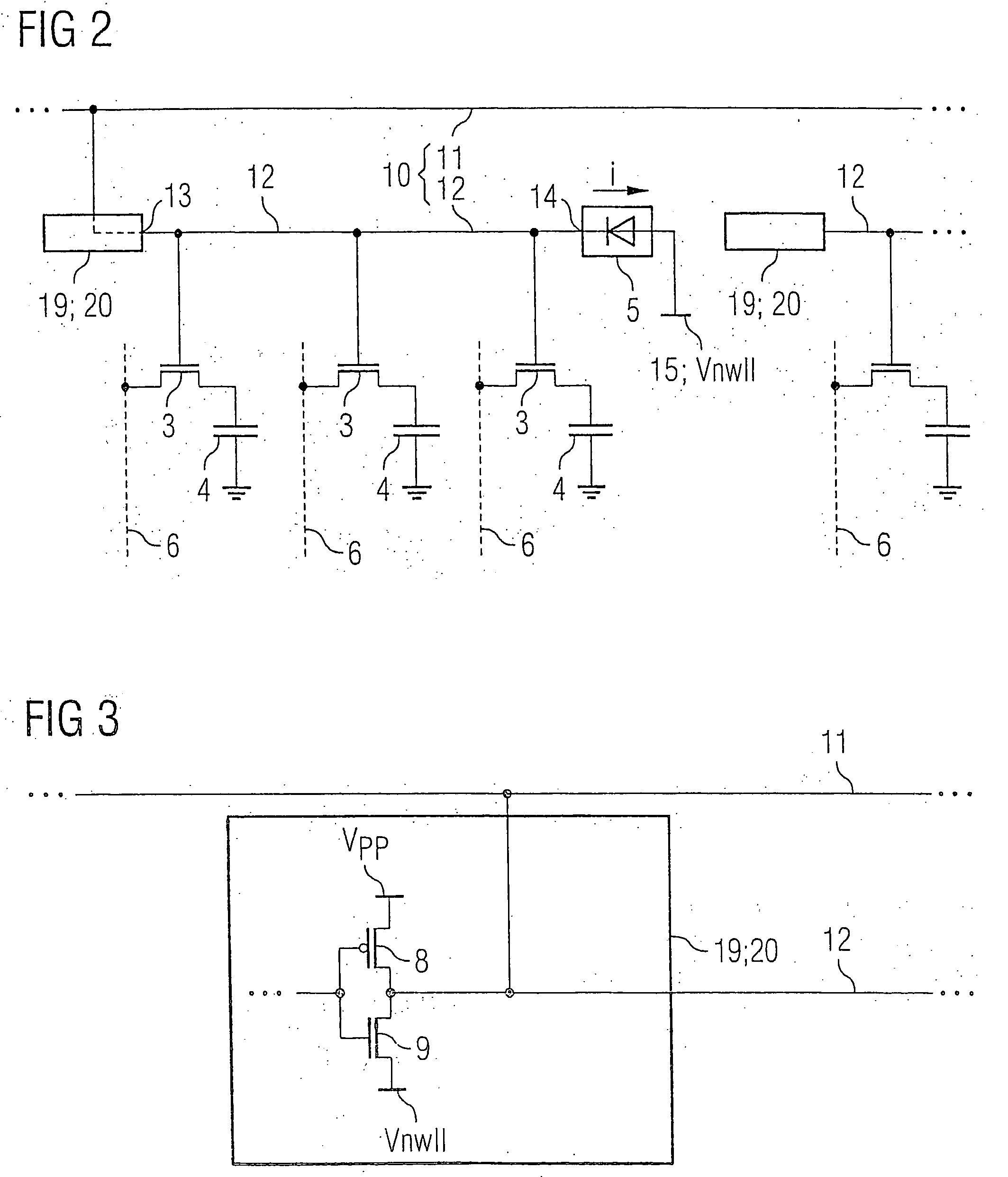
[0086]FIG. 2 shows a schematic illustration of a segmented word line of a semiconductor memory according to the invention. The segmented word line 10 has a master word line 11 and a multiplicity of conductor segments 12, which are electrically connected to the master word line. The electrical connection between the master word line and the conductor segment may be produced by means of a conductive contact hole filling (stitch) or by means of an active word line driver s...


PUM


Abstract

An integrated semiconductor memory includes at least one word line and a number of memory cells. Each memory cell has a selection transistor coupled to the word line. A word line driver is coupled to the word line. The word line driver provides a first electrical potential or a second electrical potential to the word line such that the word line is activated by the first electrical potential and is deactivated by the second electrical potential. A passive component (e.g., a diode or a resistor) is coupled between the word line and the second electrical potential such that the word line is coupled to the second electrical potential in a high-resistance fashion through the passive component. The passive component is transmissive for a leakage current between the word line and the contact connection.

Description

[0001] This application claims priority to German Patent Application 10 2004 026 128.8, which was filed May 28, 2004, and is incorporated herein by reference. TECHNICAL FIELD [0002] The invention relates to an integrated semiconductor memory comprising at least one word line and comprising a multiplicity of memory cells. BACKGROUND [0003] In integrated semiconductor memories, digital information items are stored in a multiplicity of memory cells that are in each case connected to a bit line and to a word line. Volatile semiconductor memories, in particular DRAMs (dynamic random access memory), possess memory cells that in each case have a selection transistor and a storage capacitor. The storage capacitor may be designed as a trench capacitor or as a stacked capacitor. One electrode of the storage capacitor can be electrically connected to a bit line by the selection transistor. By means of the bit line, a digital information item can be written to the storage capacitor or be read o...

Claims


Application Information

Patent Timeline
Patent Type & Authority Applications(United States)
IPC IPC(8): G11C8/00G11C8/08G11C11/407G11C11/408G11C29/00G11C29/02H10B12/00
CPCG11C11/4085G11C29/02G11C29/025H01L27/10897G11C29/832G11C2029/1202H01L27/10891G11C29/83H10B12/488H10B12/50
Inventor KLIEWER, JORGBENZINGER, HERBERTPROLL, MANFREDSCHRODER, STEPHAN
Owner POLARIS INNOVATIONS
Learn More