
Small dimension high-efficiency high-speed vertical-cavity surface-emitting lasers

a laser and surface-emitting laser technology, applied in semiconductor lasers, instruments, program control, etc., can solve problems such as unsatisfactory optical scattering, and achieve the effects of reducing mode volume, minimal added loss, and reducing parasitics

Active Publication Date: 2011-03-29
RGT UNIV OF CALIFORNIA
View PDF0 Cites 8 Cited by
  • Summary
  • Abstract
  • Description
  • Claims
  • Application Information

AI Technical Summary

Benefits of technology

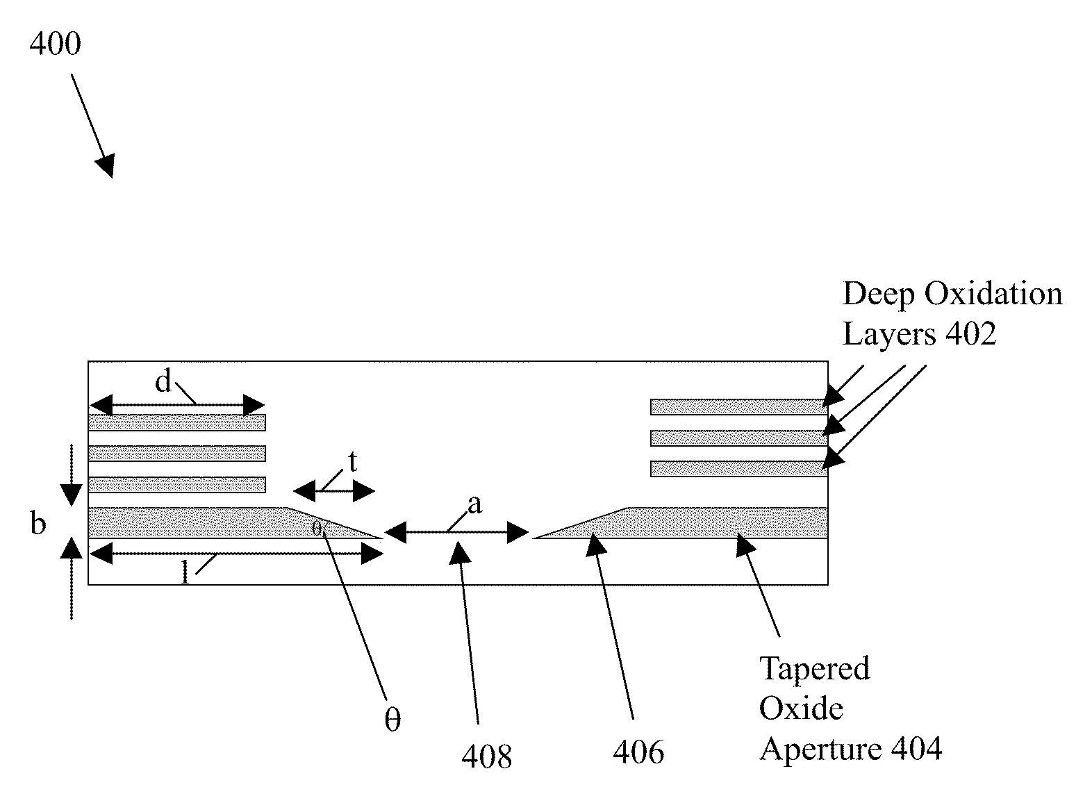
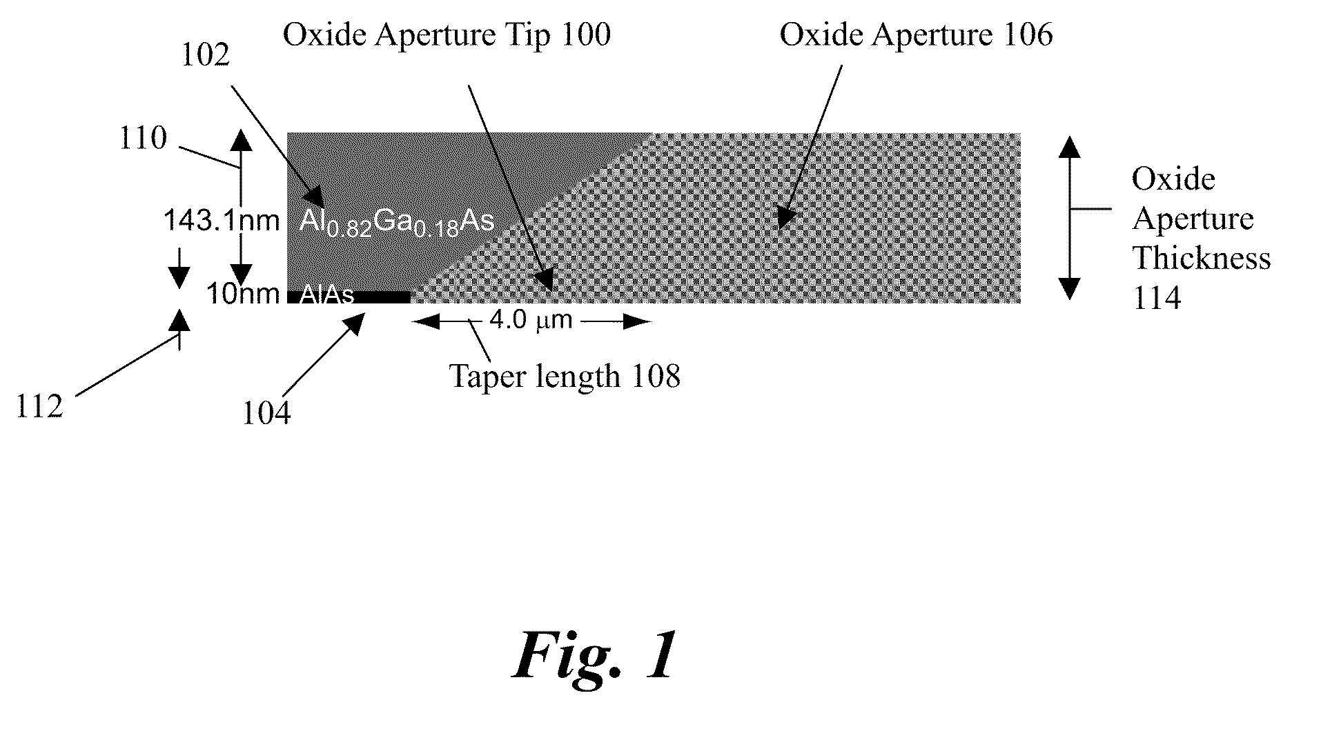
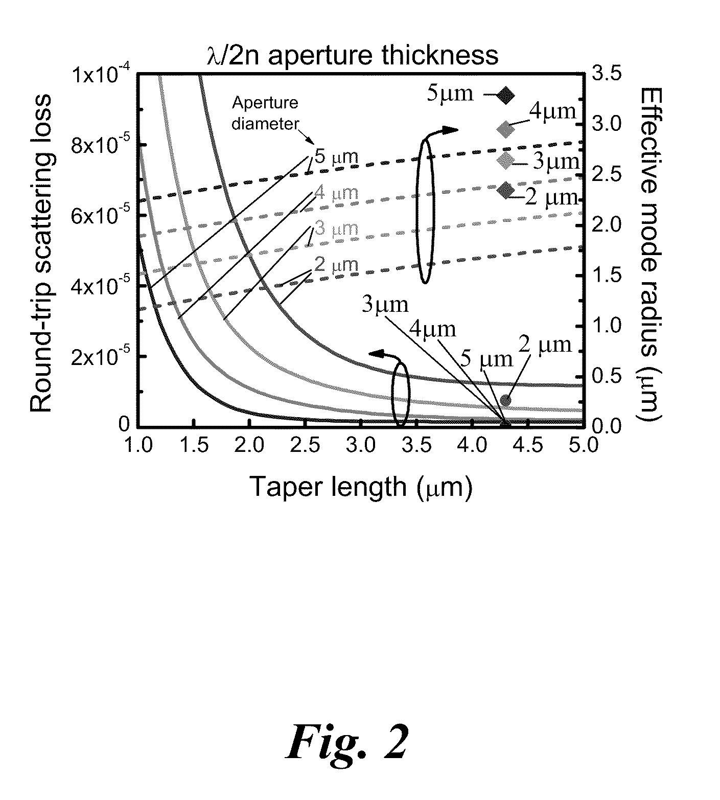
The present invention aims to reduce or eliminate the parasitic effect in VCSELs by using properly engineered apertures to enable smaller mode diameters with minimal added loss. By using a thicker oxide aperture with tapered tips, the mode volume can be reduced with minimal added loss. The invention also includes a method of fabricating a VCSEL with increased modulation bandwidth by designing a thickness, a taper length, an aperture length, a taper angle, and an aperture opening diameter that reduces the optical mode's diameter without significantly increasing the optical mode's round-trip scattering loss. The invention can achieve higher intrinsic modulation bandwidth with lower power dissipation.

Problems solved by technology

However, in the prior art these apertures have produced undesirable optical scattering due to their imperfect shape [1,2], and a larger mode diameter is needed for low optical loss.

Method used


Image

  • Small dimension high-efficiency high-speed vertical-cavity surface-emitting lasers
  • Small dimension high-efficiency high-speed vertical-cavity surface-emitting lasers
  • Small dimension high-efficiency high-speed vertical-cavity surface-emitting lasers

Examples


Embodiment Construction

ic cross-section of a VCSEL according to the present invention, FIG. 5(b) is a schematic top view of an optical mode of FIG. 5(a), showing the optical mode diameter and a Gaussian TEM00 shape, and FIG. 5(c) is an SEM image of the top of the VCSEL in FIG. 5(a).

[0025]FIG. 6 is a flowchart illustrating a method of the present invention.

[0026]FIG. 7 is a bit error rate (BER) measurement of a VCSEL of the present invention, plotting log BER vs. received power (power in dBm), for a VCSEL bias current Ibias of 4.4 milliamps (mA), a voltage swing Vac of 0.84 V peak to peak (Vp-p), wherein the inset is an optical eye diagram at 35 Gbit / s with an open eye showing an extinction ratio (ER) of 5.4 dB.

[0027]FIG. 8 plots frequency response (dB) as a function of frequency (GHz) for a 3 μm diameter device under 0.3 mA, 0.6 mA, 0.9 mA, and 1.2 mA bias currents and at a temperature of 20 degrees Celsius.

DETAILED DESCRIPTION OF THE INVENTION

[0028]In the following description of the preferred embodiment...


PUM


Abstract

A Vertical-Cavity Surface-Emitting Laser (VCSEL) is disclosed, comprising an optical cavity bounded by a top mirror and a bottom mirror, wherein the top mirror has multiple layers of alternating refractive index, of which the bottom three or more layers of the top mirror are deep oxidation layers having an increased oxidation length, a light emitting active region between the top mirror and the bottom mirror, and an aperture with tapered edges between the active region and the top mirror, wherein the aperture has a thickness, a taper length, an oxide aperture length, a taper angle, and an aperture opening diameter designed to reduce an optical mode's diameter without significantly increasing the optical mode's round trip scattering loss.

Description

CROSS REFERENCE TO RELATED APPLICATIONS[0001]This application claims the benefit under 35 U.S.C. Section 119(e) of commonly-assigned U.S. Provisional Patent Application Ser. No. 61 / 039,048, filed on Mar. 24, 2008, by Yu-Chia Chang and Larry A. Coldren, entitled “SMALL DIMENSION HIGH EFFICIENCY HIGH-SPEED VERTICAL-CAVITY SURFACE-EMITTING LASERS,” which application is incorporated by reference herein.BACKGROUND OF THE INVENTION[0002]1. Field of the Invention[0003]This invention relates to improved performance apertures and mirrors for Vertical-Cavity Surface-Emitting Lasers (VCSELs).[0004]2. Description of the Related Art[0005](Note: This application references a number of different publications as indicated throughout the specification by one or more reference numbers within brackets, e.g., [x]. A list of these different publications ordered according to these reference numbers can be found below in the section entitled “References.” Each of these publications is incorporated by refe...

Claims


Application Information

Patent Timeline
Patent Type & Authority Patents(United States)
IPC IPC(8): H01S5/00
CPCH01S5/18305H01S5/18333H01S5/028H01S5/06226H01S5/18311H01S2301/166
Inventor CHANG, YU-CHIACOLDREN, LARRY A.
Owner RGT UNIV OF CALIFORNIA
Learn More