Oscillation device
a technology of oscillating device and oscillating axis, which is applied in the direction of optical radiation measurement, pulse technique, instruments, etc., to achieve the effect of high-speed information communication
- Summary
- Abstract
- Description
- Claims
- Application Information
AI Technical Summary
Benefits of technology
Problems solved by technology
Method used
Image
Examples
example 1
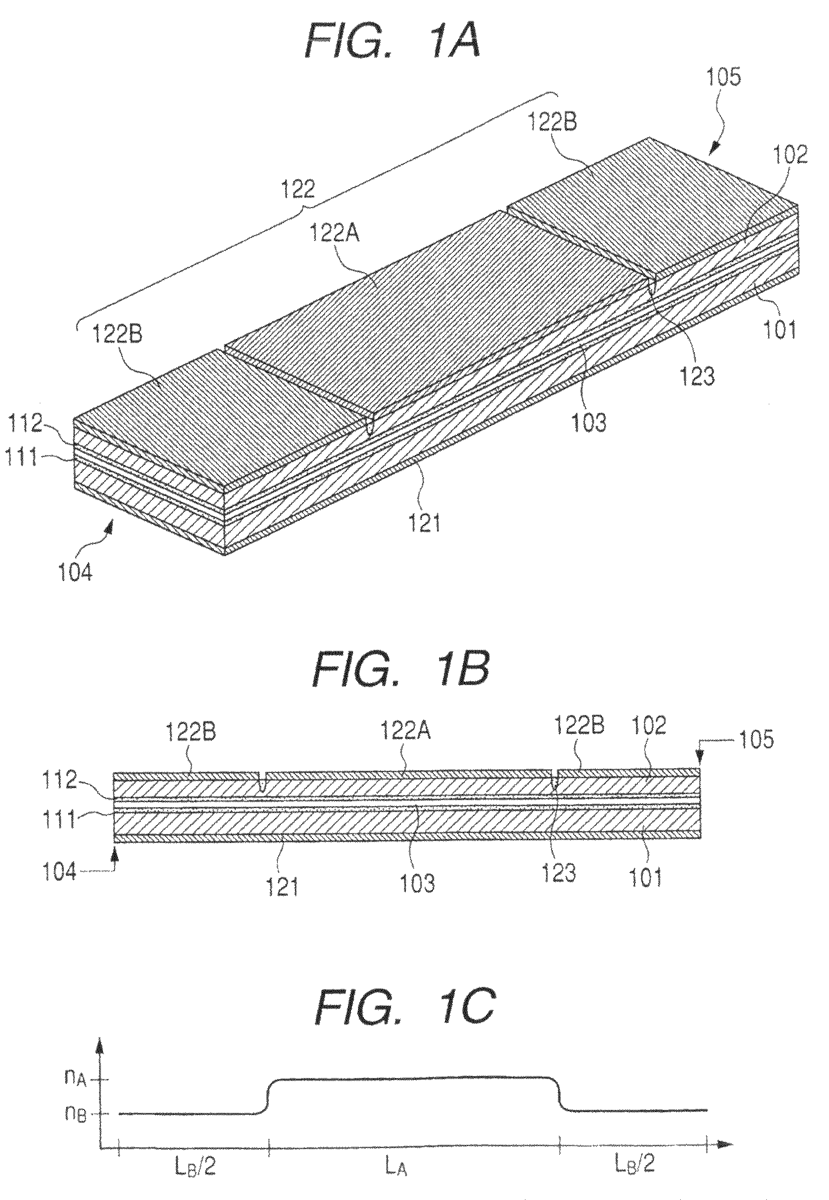
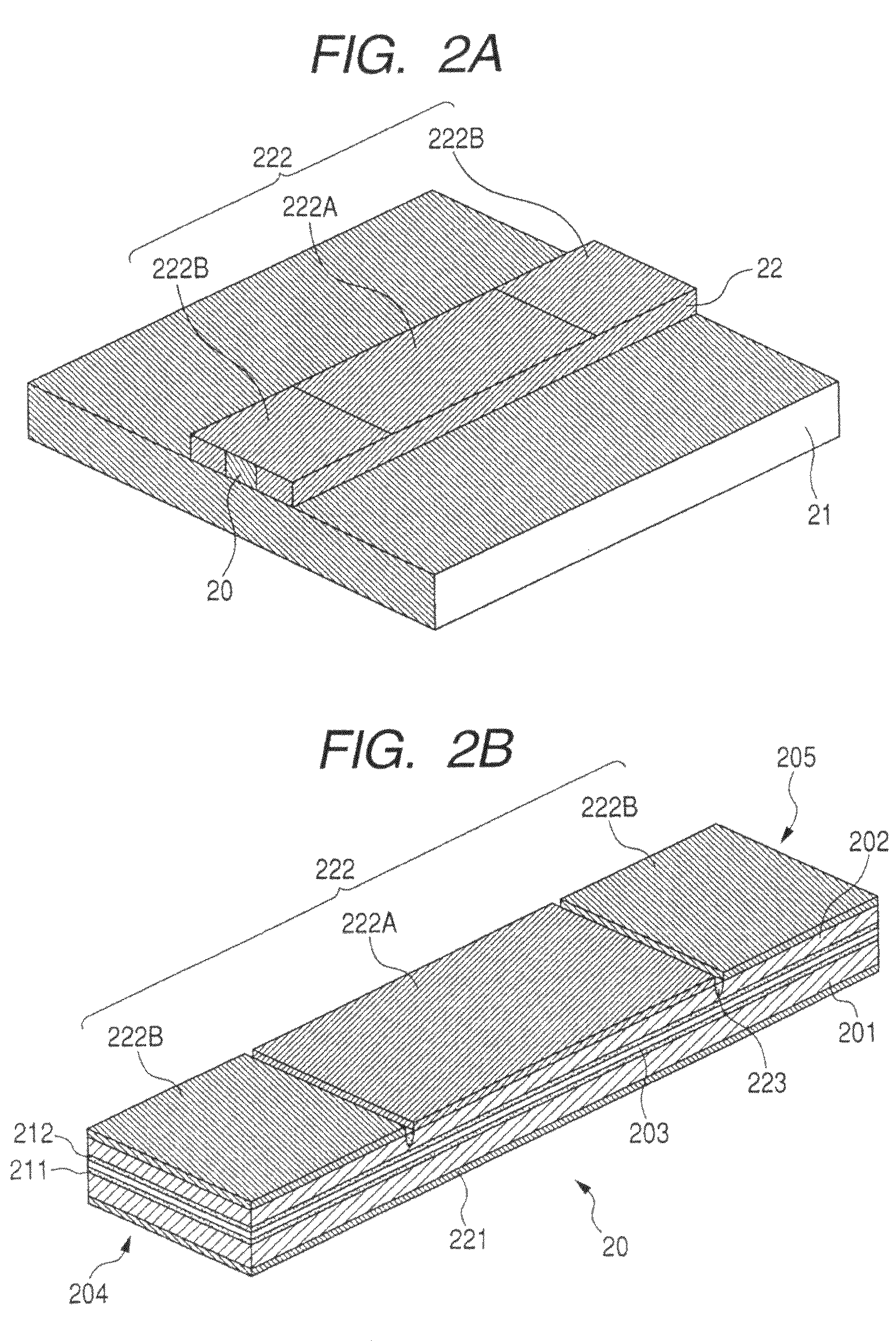
[0042]FIGS. 2A and 2B illustrate a first example of an oscillation device to which the present invention is applied. FIG. 2B illustrates, in an enlarged manner, a device body 20 illustrated in FIG. 2A. In this example, a gain medium is a resonant tunneling diode (RTD) based on photon-assisted tunneling. Gain produced in the RTD is observed as negative resistance in DC. In this case, it is considered that the gain broadly extends from millimeter wave band up to terahertz band. Accordingly, the RTD is a desirable example as a gain medium forming an oscillation device to which the present invention can be applied.
[0043]In FIG. 2B, a gain medium 203 is an RTD, and is of the configuration in which three barrier layers are used like spacer layer / barrier layer / well layer / barrier layer / well layer / barrier layer / spacer layer, for example. In order to realize this configuration, lattice-matched InGaAs may be used on InP substrate as well layer, and lattice-matched InAlAs or non-matched AlAs ma...
example 2
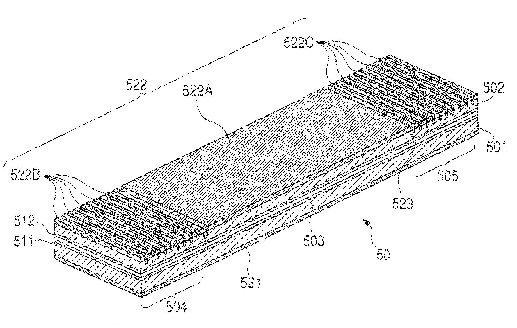
[0058]FIGS. 5A and 5B illustrate the configuration of the second example of an oscillation device to which the present invention is applied. FIG. 5B shows, in an enlarged manner, the device body in FIG. 5A. In this example, the cavity structure uses DBR. Since the cavity structure having wavelength selectivity is employed as the cavity structure differently from Example 1, mode hopping becomes difficult to take place. Accordingly, as cavity structure forming the oscillation device to which the present invention can be applied, this example is a more desirable example.
[0059]In FIG. 5B, an RTD on the same InP substrate as that of Example 1 is used as a gain medium 503. Electrical contacts 511 and 512 are configured so as to include a semiconductor film of n-InGaAs (thickness 50 nm) having electron concentration of 1×1018 cm−3, and negative permittivity media 501, 502 are configured so as to include a semiconductor film of n-InGaAs (thickness 100 nm) having electron concentration of 1×...
example 3
[0066]FIGS. 6A and 6B illustrate the configuration of an oscillation device of the third example to which the present invention is applied. FIG. 6B illustrates, in an enlarged manner, a device body 60 in FIG. 6A. In the present example, a gain medium is a resonant inter-band tunneling diode (RITD) based on photon-assisted tunneling. The RITD has a gain of millimeter wave band utilizing the photon-assisted tunneling. Accordingly, there is disclosed a modified example of a gain medium forming an oscillation device to which the present invention can be applied.
[0067]In FIG. 6B, a gain medium 603 is RITD, and is of the configuration using Type II hetero-junction, e.g., as in the case of n type 8 doped part / spacer layer / Type II spacer layer / p-type 8 doped part / Type II p-type layer. In connection with these components, lattice-matched Si may be used on an Si substrate as a spacer layer, and SiGe which is non-matched and serves as Type II hetero-junctioned to Si may be used as a Type II sp...
PUM
 Abstract
Description
Claims
Application Information
 - R&D
- Intellectual Property
- Life Sciences
- Materials
- Tech Scout
- Unparalleled Data Quality
- Higher Quality Content
- 60% Fewer Hallucinations
Browse by: Latest US Patents, China's latest patents, Technical Efficacy Thesaurus, Application Domain, Technology Topic, Popular Technical Reports.
© 2025 PatSnap. All rights reserved.Legal|Privacy policy|Modern Slavery Act Transparency Statement|Sitemap|About US| Contact US: help@patsnap.com


