Organic electroluminescent compounds and organic electroluminescent device using the same
a technology of organic electroluminescent devices and electroluminescent compounds, which is applied in the direction of discharge tube luminescnet screens, organic chemistry, natural mineral layered products, etc., can solve the problems of difficult application of materials to display of high quality, urgent research and development of such materials, and merely a few thousand hours of life. , to achieve the effect of excellent luminous efficiency and improved lifetim
- Summary
- Abstract
- Description
- Claims
- Application Information
AI Technical Summary
Benefits of technology
Problems solved by technology
Method used
Image
Examples
preparation examples
Preparation Example 1
[0122]Preparation of Compound (1)
[0123]
[0124]Preparation of Compound (A)
[0125]Under nitrogen atmosphere, a 50 mL round-bottomed flask was charged with 3-bromopyridine (96 μL, 1 mmol) and diethyl ether (10 mL), and the mixture was stirred. After chilling to −78° C., butyllithium (2.5 mL, 1 mmol, 2.5 M in hexane) was slowly added thereto. The resultant mixture was stirred at −78° C. for 1 hour, and dimethyl phthalate (0.17 mL, 1 mmol) was slowly added at −78° C. After stirring at the same temperature for 2 hours, the temperature was slowly raised to room temperature, and water (5 mL) was added to the reaction mixture to carry out hydrolysis. Organic layers obtained from ether extraction were combined, and dried to remove the solvent. Purification via column chromatography gave Compound (A) (0.14 g, 56%) as solid product.
[0126]Preparation of Compound (B)
[0127]Under nitrogen atmosphere, a 50 mL round-bottomed flask was charged with Compound (A) (0.11 g, 0.44 mmol) a...
example 1
Manufacture of an OLED Employing Organic Electroluminescent Compound According to the Invention
[0140]An OLED device was manufactured by using an electroluminescent material according to the invention.
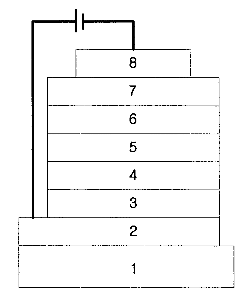
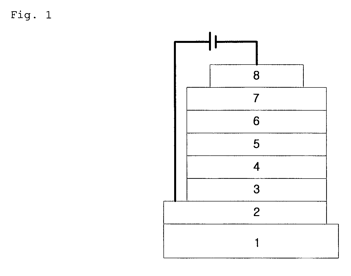
[0141]First, a transparent electrode ITO thin film (15Ω / □) (2) prepared from glass for OLED (produced by Samsung Corning) (1) was subjected to ultrasonic washing with trichloroethylene, acetone, ethanol and distilled water, sequentially, and stored in isopropanol before use.
[0142]Then, an ITO substrate was equipped in a substrate folder of a vacuum vapor-deposit device, and 4,4′,4″-tris(N,N-(2-naphthyl)-phenylamino)triphenylamine (2-TNATA) was placed in a cell of the vacuum vapor-deposit device, which was then ventilated up to 10−6 torr of vacuum in the chamber. Electric current was applied to the cell to evaporate 2-TNATA, thereby providing vapor-deposit of a hole injecting layer (3) having 60 nm of thickness on the ITO substrate.
[0143]
[0144]Then, to another cell of the vacuum vapor-de...
example 2
Manufacture of an OLED by Using a Compound According to the Present Invention
[0154]After forming a hole injecting layer and a hole transport layer according to the same procedure as described in Example 1, a compound according to the present invention (e.g. Compound 5) was charged to one cell of said vacuum vapor-deposit device as electroluminescent material, and Compound (E) (of which the structure is shown below) was charged to another cell. Then the two materials were evaporated at different rates to carry out doping at a concentration of 2 to 5% by weight on the basis of the host, thereby providing an electroluminescent layer having 30 nm of thickness vapor-deposited on the hole transport layer.
[0155]
[0156]Then, an electron transport layer and electron injecting layer were vapor-deposited according to the same procedure as in Example 1, and an Al cathode was vapor-deposited thereon with a thickness of 150 nm by using another vacuum vapor-deposit device to manufacture an OLED.
PUM
| Property | Measurement | Unit |
|---|---|---|
| external quantum efficiency | aaaaa | aaaaa |
| electroluminescent peak of wavelength | aaaaa | aaaaa |
| temperature | aaaaa | aaaaa |
Abstract
Description
Claims
Application Information
 - R&D
- Intellectual Property
- Life Sciences
- Materials
- Tech Scout
- Unparalleled Data Quality
- Higher Quality Content
- 60% Fewer Hallucinations
Browse by: Latest US Patents, China's latest patents, Technical Efficacy Thesaurus, Application Domain, Technology Topic, Popular Technical Reports.
© 2025 PatSnap. All rights reserved.Legal|Privacy policy|Modern Slavery Act Transparency Statement|Sitemap|About US| Contact US: help@patsnap.com


