Method for manufacturing semiconductor substrate

a manufacturing method and semiconductor technology, applied in semiconductor/solid-state device manufacturing, basic electric elements, electric instruments, etc., can solve the problems of easy generation of defect levels, increase of defects in poor characteristics of semiconductor elements manufactured using single crystal semiconductor layers, etc., to achieve favorable and uniform characteristics, reduce in-plane variation of semiconductor layers, and improve productivity

Inactive Publication Date: 2011-02-08
SEMICON ENERGY LAB CO LTD
View PDF11 Cites 2 Cited by
  • Summary
  • Abstract
  • Description
  • Claims
  • Application Information

AI Technical Summary

Benefits of technology

[0011]As an alternative method, a method in which a single crystal semiconductor layer is irradiated with laser light is given, for example. By irradiation with laser light, only the single crystal semiconductor layer can be selectively melted, whereby defects can be reduced. As the laser light, pulsed laser light is typically used. The pulsed laser light has the advantage that light intensity that is needed for melting can be obtained more easily than in the case of using continuous-wave laser light.
[0019]In the above description, the expression “conditions where the semiconductor layer is not melted” refers to conditions where volume movement resulting from melting does not occur, but the expression does not exclude conditions where instantaneous melting occurs while volume movement does not occur, conditions where microscopic bond rearrangement occurs, and the like. In this sense, the above expression “under conditions where the semiconductor layer is not melted” can be replaced with the expression “under conditions where the planarity of the surface of the semiconductor layer is not changed.” In other words, the intensity of the light from the flash lamp may be controlled such that the unevenness of the surface of the semiconductor layer does not change.
[0023]In one embodiment of the disclosed invention, light from a flash lamp (hereinafter also referred to as flash lamp light) is used to repair defects of a semiconductor layer without melting the semiconductor layer. Thus, compared to the case of using laser light and melting a semiconductor layer, productivity can be drastically improved. In addition, since a semiconductor layer is not melted, a crystal grain boundary and the like resulting from generation of a melted region and an unmelted region are not produced. Thus, in-plane variation of a semiconductor layer can be reduced, and a semiconductor layer having favorable and uniform characteristics can be obtained. Furthermore, compared to heating in thermal equilibrium with a furnace or the like, treatment can be efficiently performed in an extremely short time. That is, a large-area substrate having favorable and uniform characteristics can be provided extremely efficiently. Note that when a semiconductor layer is irradiated with laser light to improve its characteristics, linear pulsed laser light having a beam spot of about 0.5 mm×300 mm is normally used. This is because light intensity sufficient for partial melting of the semiconductor layer is needed. On the other hand, in the present invention, flash lamp light enables a large area to be treated at a time.

Problems solved by technology

In the case where a single crystal semiconductor layer is formed by using a method in which a single crystal semiconductor substrate is irradiated with ions, the ion irradiation leads to an increase of defects in the single crystal semiconductor layer.
In the case where many such defects exist in a single crystal semiconductor layer, a semiconductor element manufactured using this single crystal semiconductor layer has poorer characteristics; for example, defect levels are easily generated at the interface with a gate insulating layer.
Further, in the case where many defects exist in a single crystal semiconductor layer, original characteristics of the single crystal semiconductor cannot be obtained.
However, heat treatment at a high temperature (e.g., 800° C. or higher) is not appropriate as treatment on a single crystal semiconductor layer formed over a glass substrate.
This is because a glass substrate has an issue about allowable temperature limit.
Here, in the case of irradiating a single crystal semiconductor layer with laser light, there is a problem in that characteristics of the single crystal semiconductor layer are lowered in a region irradiated with an edge portion of the laser light.
This is because a melted region and an unmelted region are mixed in that region, and therefore, a distortion is easily generated in a crystal structure at a boundary between the melted region and the unmelted region.
However, it is very difficult to obtain laser light having a light intensity that enables a large-area semiconductor layer to be uniformly melted.

Method used


Image

  • Method for manufacturing semiconductor substrate
  • Method for manufacturing semiconductor substrate
  • Method for manufacturing semiconductor substrate

Examples


embodiment 1

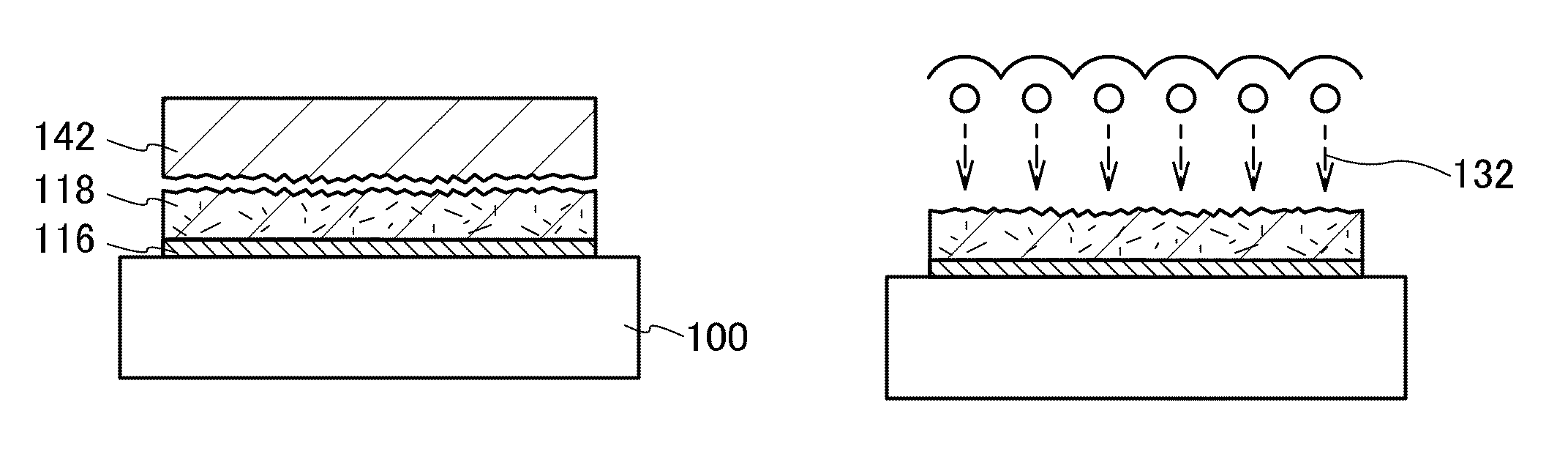
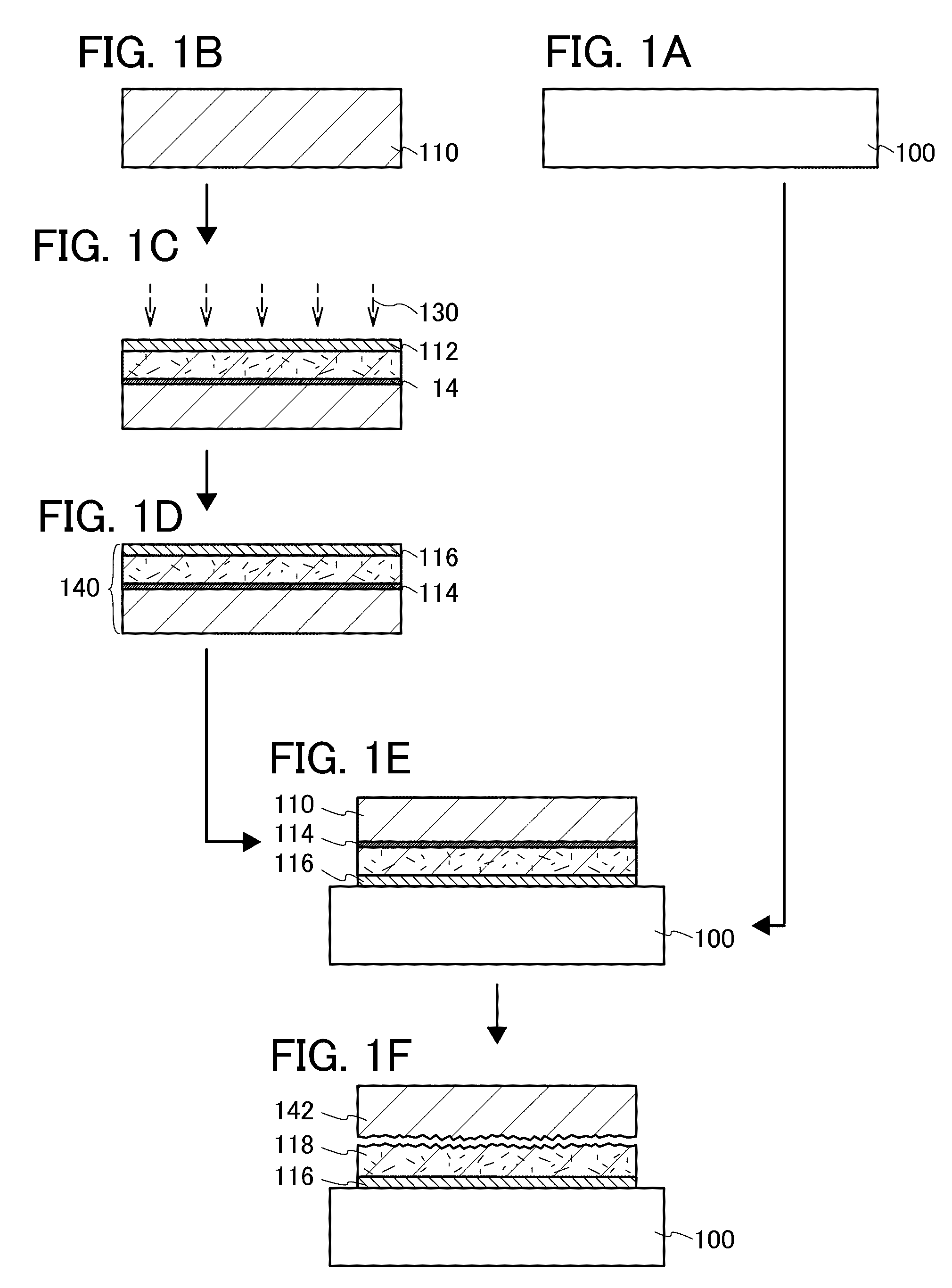
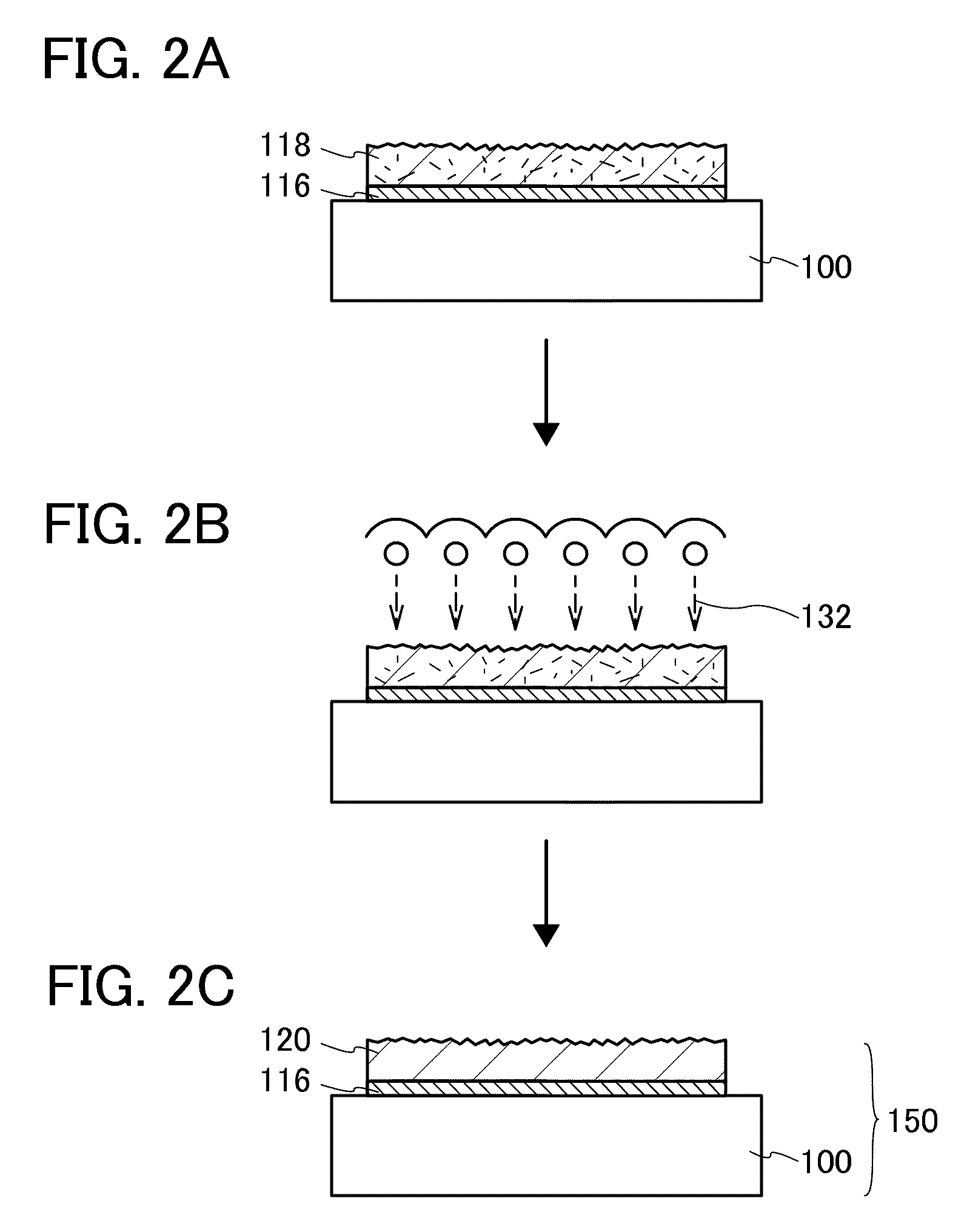
[0041]In Embodiment 1, a method for manufacturing a semiconductor substrate which is one embodiment of the disclosed invention will be described with reference to FIGS. 1A to 1F and FIGS. 2A to 2C.

[0042]First, a base substrate 100 is prepared (see FIG. 1A). As the base substrate 100, a substrate having an insulating surface, such as a visible light transmitting glass substrate used for a liquid crystal display device or the like, can be used, for example. As a glass substrate, a substrate having a strain point of 580° C. or higher (preferably, 600° C. or higher) may be used. Further, it is preferable that the glass substrate be a non-alkali glass substrate. As a material of the non-alkali glass substrate, a glass material such as aluminosilicate glass, aluminoborosilicate glass, or barium borosilicate glass is used, for example.

[0043]Note that as the base substrate 100, as well as a glass substrate, a substrate having an insulating surface, such as a ceramic substrate, a quartz subs...

embodiment 2

[0089]In Embodiment 2, a variation of the method for manufacturing a semiconductor substrate in Embodiment 1 will be described. Specifically, the case of employing planarization treatment by etching will be described with reference to FIGS. 3A to 3D and FIGS. 4A to 4D. Note that many parts of a manufacturing process of a semiconductor substrate described in this embodiment are the same as those in Embodiment 1. Thus, description of parts overlapping with those in Embodiment 1 will be omitted below, and differences will be mainly described.

[0090]First, a method illustrated in FIGS. 3A to 3D is described.

[0091]First, in accordance with the method described in Embodiment 1 or the like, a base substrate 100 and a substrate 140 are bonded together, and then, the substrate 140 is divided into a single crystal semiconductor substrate 142, and an insulating layer 116 and a semiconductor layer 118. Accordingly, a semiconductor substrate including the semiconductor layer 118 over the base sub...

embodiment 3

[0107]In Embodiment 3, another example of a method for manufacturing a semiconductor substrate of the present invention will be described with reference to FIGS. 5A to 5E and FIGS. 6A to 6C. Note that many parts of a manufacturing process of a semiconductor substrate described in this embodiment are the same as those in Embodiment 1. Thus, differences will be mainly described.

[0108]First, a base substrate 100 is prepared (see FIG. 5A). Embodiment 1 can be referred to for the details of the base substrate 100. In addition, a single crystal semiconductor substrate 110 is prepared. Embodiment 1 can be referred to also for the details of the single crystal semiconductor substrate 110.

[0109]Next, a variety of treatments are performed on the single crystal semiconductor substrate 110 to form a damaged region 114 and an insulating layer 116 (see FIG. 5B). Embodiment 1 may be referred to for the details of the variety of treatments. Note that the damaged region 114 is a region which contain...


PUM


Abstract

One surface of a single crystal semiconductor substrate is irradiated with ions to form a damaged region in the single crystal semiconductor substrate. An insulating layer is formed over the one surface of the single crystal semiconductor substrate. A surface of a substrate having an insulating surface and a surface of the insulating layer are disposed in contact with each other to bond the substrate having the insulating surface and the single crystal semiconductor substrate to each other. Heat treatment is performed to divide the single crystal semiconductor substrate along the damaged region and to form a semiconductor layer over the substrate having the insulating surface. One surface of the semiconductor layer is irradiated with light from a flash lamp under conditions where the semiconductor layer is not melted, to repair a defect.

Description

BACKGROUND OF THE INVENTION[0001]1. Field of the Invention[0002]A technical field of the present invention relates to a method for manufacturing a semiconductor substrate.[0003]2. Description of the Related Art[0004]In recent years, semiconductor devices formed using an SOI (silicon on insulator) substrate, instead of a bulk silicon substrate, have been developed. By utilizing the features of a thin single crystal silicon layer formed over an insulating layer, transistors in a semiconductor device can be completely isolated from each other, and further, fully depleted transistors can be formed. Accordingly, a semiconductor integrated circuit with high added values such as high integration, high speed driving, and low power consumption can be realized.[0005]As a method for manufacturing an SOI substrate, a so-called hydrogen-ion-implantation separation method is known. A typical process of the method will be described below.[0006]First, hydrogen ions are implanted into a silicon subs...

Claims


Application Information

Patent Timeline
Patent Type & Authority Patents(United States)
IPC IPC(8): H01L21/30
CPCH01L21/76254
Inventor TANAKA, KOICHIRO
Owner SEMICON ENERGY LAB CO LTD
Why Eureka
Try Eureka