
Transparent electrically conductive film and process for producing the same

a technology of electrical conductivity and transparent film, which is applied in the direction of photosensitive materials, conductive layers on insulating supports, instruments, etc., can solve the problems of increasing production costs, affecting the quality of electrical conductivity, and unable to afford satisfactory electromagnetic wave shielding properties, etc., to achieve excellent electrical conductivity, reduce the number of manufacturing steps, and produce in high yield and inexpensively.

Inactive Publication Date: 2011-02-08
SEIREN CO LTD
View PDF11 Cites 2 Cited by
  • Summary
  • Abstract
  • Description
  • Claims
  • Application Information

AI Technical Summary

Benefits of technology

[0010]According to the present invention it is possible to provide an electrically conductive film which, while maintaining the light transparency of a transparent film, has excellent electrical conductivity and can be utilized for electromagnetic wave shielding. Further, it is possible to provide a transparent, electrically conductive film free from separation of a metal layer and inclusion of air bubbles when laminated to another base material and which can be produced in high yield and inexpensively through a reduced number of manufacturing steps.

Problems solved by technology

The above transparent, electrically conductive film having ITO film on a transparent substrate is superior in light transparency, but is inferior in electrical conductivity and cannot afford satisfactory electromagnetic wave shielding properties in comparison with the transparent, electrically conductive film having a mesh-like thin metal film.
On the other hand, in the process involving forming a thin metal film on a transparent substrate and processing it into mesh-like, since most of the thin metal film is removed, this is wasteful and results in an increase of the production cost, although there is attained high electrical conductivity.
According to this process, however, it is difficult to prepare a pattern using thin lines not larger than 30 μm in line width, and a large line width results in deterioration of light transparency; besides, when the transparent, electrically conductive film formed by this process is used as an electromagnetic wave shielding material for display, it is inferior in image visibility.
In this case, in the transparent, electrically conductive film formed by the above process, the ink layer after printing is thick and concaves and convexes on the print surface are large, so when the adhesive is applied to the surface of one film and this film is laminated to the other film, there easily occurs inclusion of air bubbles and image visibility is deteriorated in the presence of such air bubbles.

Method used


Image

  • Transparent electrically conductive film and process for producing the same
  • Transparent electrically conductive film and process for producing the same

Examples


examples

[0035]The present invention will be described below in more detail by way of examples, but the invention is not limited to the following examples. Transparent, electrically conducive films produced by the following working and comparative examples were evaluated in the following manner.

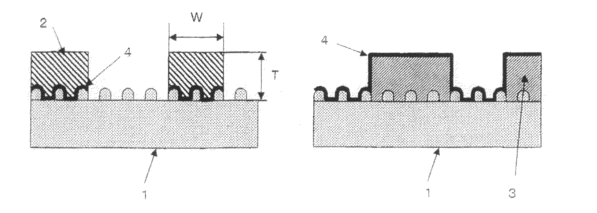
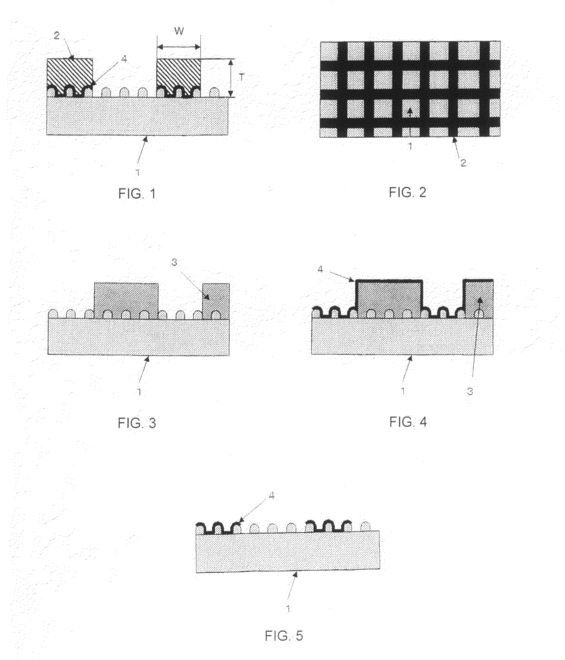
(1) Concaves / Convexes of Film and Height T of Metal Layer

[0036]A part of film was cut out and a thin piece thereof was cut out in a sectional direction with a microtome, then was observed and measured using a laser microscope (LEXT OLS3000, a product of Olympus Co., Ltd.).

(2) Width W of Metal Layer

[0037]The width of a metal layer of a transparent, electrically conductive film was measured from a surface of the same layer with use of a laser microscope (LEXT OLS3000, a product of Olympus Co., Ltd.).

(3) Electrical Conductivity

[0038]Measured using LORESTA AP (4-pin probe method) (a product of Mitsubishi Chemical Co., Ltd.).

(4) Transmittance

[0039]The transmittance of light (visible light) having a wavelen...

example 2

[0041]A layer containing alumina (refractive index 1.56) with an average particle diameter of 0.1 m was laminated to a surface of a PET film (light transmittance 92%, refractive index 1.55) to afford a transparent film having concaves and convexes with an average height of 0.05 μm. Then, a photosensitive resist (PER20 SC03, a product of Taiyo Ink Mfg. Co., Ltd.) was applied onto the film surface to a thickness of 10 μm, followed by exposure and development, to afford a film having 300×300 μm resist blocks arranged at 20 μm intervals. Next, the film was subject to electroless copper plating in the same way as in Example 1 to afford a transparent, electrically conductive film. This film was then subjected to electrolytic copper plating to afford a transparent, electrically conductive film according to the present invention having a metal layer width W of 20 μm, a metal layer thickness of 5 μm and a W / T ratio of 4. An EVA adhesive was applied to the surface of the transparent, electric...

example 3

[0042]A layer containing silica (refractive index 1.46) with an average particle diameter of 0.1 μm was laminated to a surface of a PET film (light transmittance 92%, refractive index 1.55) to afford a transparent film having concaves and convexes with an average height of 0.05 μm. Then, a photosensitive resist (PER20m SC03, a product of Taiyo Ink Mfg. Co., Ltd.) was applied onto the film surface to a thickness of 10 μm, followed by exposure and development, to afford a film having 100×100 μm resist blocks arranged at 50 μm intervals. Next, the film was subjected to electroless copper plating in the same way as in Example 1 to afford a transparent, electrically conductive film according to the present invention having a metal layer width W of 50 μm, a metal layer thickness T of 0.1 μm and a W / T ratio of 500. A EVA adhesive was applied to the surface of the transparent, electrically conductive film and a PET film having a reflection preventing layer was laminated thereto.


PUM

PropertyMeasurementUnit
heightaaaaaaaaaa
refractive indexaaaaaaaaaa
thicknessaaaaaaaaaa

Abstract

This invention provides a transparent electrically conductive film, which, while maintaining the light transparency of a transparent film, has excellent electrical conductivity, can be utilized for electromagnetic wave shielding, and does not cause inclusion of air bubbles in the lamination onto other base material, and a process for producing the same. The production process comprises the steps of forming a large number of concaves and convexes having an average height of not more than 0.1 μm on both sides or one side of a transparent film, forming a resist layer having a pattern shape opposite to the electrically conductive part in the electrically conductive film on the transparent film on its concave-convex side, applying a catalyst for plating onto the resist layer-formed face, separating the resist layer, forming a metal layer by plating, and blackening the metal layer, the metal layer satisfying 1≦W / T≦500 wherein W represents the width of the metal layer and T represents the height of the metal layer.

Description

FIELD OF THE INVENTION[0001]The present invention relates to a transparent, electrically conductive film as a light transmitting electromagnetic wave shielding material for use in a filter disposed on a front display surface of, for example, a CRT or a plasma display panel or in a display part of a measuring instrument, as well as a process for producing such a film. More particularly, the present invention is concerned with a transparent, electrically conductive film having an electromagnetic wave shielding function and which permits a user to see through the interior of, for example, a microwave oven or a measuring instrument or a display surface of, for example, a CRT or a plasma display panel.BACKGROUND OF THE INVENTION[0002]As conventional processes for producing an electrically conductive film which can shield electromagnetic waves while maintaining satisfactory light transparency there are known, for example, a process in which a transparent, electrically conductive film such...

Claims


Application Information

Patent Timeline
Patent Type & Authority Patents(United States)
IPC IPC(8): G03F1/00H01L21/00B32B15/08H01B5/14H01B13/00H05K9/00
CPCB32B27/00H05K9/0096H05K3/185H05K2203/0565H05K2203/1415H05K9/00H01B5/14H01J11/44B32B15/08
Inventor YAMADA, KOHEISHIOMI, HIDEKAZUYAMADA, HIDEYUKI
Owner SEIREN CO LTD
Learn More