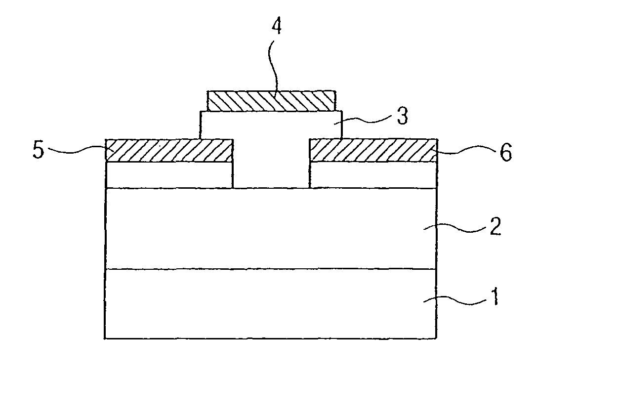
Field effect transistor
a field effect transistor and transistor technology, applied in the field of field effect transistors, can solve the problems that the transistor using silicon thin film cannot be directly formed on a less heat-resistant resin substrate, and the transistor has not been obtained which satisfies
- Summary
- Abstract
- Description
- Claims
- Application Information
AI Technical Summary
Benefits of technology
Problems solved by technology
Method used
Image
Examples
first embodiment
Transparent S,D,G Electrodes or Laminated Electrodes
[0080]The field-effect transistor of this embodiment belongs to the category of the aforementioned first, second, and third aspects of the invention.
[0081]The description “transparent to visible light” signifies a state in which the material is transparent to at least a part of the visible light wavelength region. The transparency signifies a state of not only no light absorption but also penetration of a part of the visible light. In the present invention, the transmittance of visible light is not lower than 40%, more preferably not lower than 60%, still more preferably not lower than 80%.
[0082]Thus, a highly transparent device is realized by making transparent at least a portion of the electrode or another member constituting the transistor.
[0083]Desirably, all of the source electrode, the drain electrode, the gate electrode, and the gate-insulating film are transparent to the visible light. Examples of electrodes transparent to ...
second embodiment
Multilayered Gate Insulator
[0088]The field effect transistor of this embodiment belongs to the category of the above fourth and fifth aspects of the invention. The active Layer of this embodiment is preferably constituted of an transparent amorphous oxide containing at least In—Ga—Zn—O, represented by InGaO3(ZnO)m (m: a natural number of less than 6) in a crystal state, containing carriers at a concentration of less than 1×10¹⁸ / cm3; or a transparent amorphous oxide containing In—Ga—Zn—Mg—O, represented by InGaO3(Zn1−xMgxO)n (m: a natural number of less than 6; 0<x≦1) in a crystal state.
[0089]The first layer constituting the gate-insulating film is constituted of, for example, HfO2′ or Y2O3, or a mixed crystal compound thereof. The second layer is constituted, for example, of SiO2, Si3N4, TiO2, Ta2O5, PbTiO3, BaTa2O6, SrTiO3, MgO, or AlN, or an amorphous structure containing the above substance.
[0090]The above materials of the first layer and the second layer are examples, and the ma...
third embodiment
Passivation, Surface-Coating Layer
[0121]The field-effect transistor of this embodiment belongs to the category of the above seventh, eighth and ninth aspects of the invention.
[0122]The passivation layer in the fifth aspect includes two conceptions. The passivation layer of a first conception is a separate layer provided between the active layer and the gate-insulating layer and constituted of a material different from that of the active layer or the gate-insulating layer. This passivation layer of the first concept is hereinafter referred to a “passivated layer”. The passivated layer is composed, for example, of amorphous silicon oxide, amorphous silicon nitride, titanium oxide, aluminum oxide, magnesium oxide, or the like.
[0123]The passivation layer of a second conception is an outermost surface portion of the active layer treated with oxygen plasma. The treatment for formation of the passivation layer of the second conception is hereinafter referred to as “passivation treatment”. ...
PUM
 Abstract
Description
Claims
Application Information
 - R&D
- Intellectual Property
- Life Sciences
- Materials
- Tech Scout
- Unparalleled Data Quality
- Higher Quality Content
- 60% Fewer Hallucinations
Browse by: Latest US Patents, China's latest patents, Technical Efficacy Thesaurus, Application Domain, Technology Topic, Popular Technical Reports.
© 2025 PatSnap. All rights reserved.Legal|Privacy policy|Modern Slavery Act Transparency Statement|Sitemap|About US| Contact US: help@patsnap.com


