
Internal charge transfer for circuits

a charge transfer and circuit technology, applied in the field of circuits, can solve the problems of not allowing circuit level control of stand-by operation, and achieve the effects of accelerating the transition time of sleep mode, reducing external power involvement, and fast transition

Active Publication Date: 2010-09-28
GLOBALFOUNDRIES US INC
View PDF13 Cites 4 Cited by
  • Summary
  • Abstract
  • Description
  • Claims
  • Application Information

AI Technical Summary

Benefits of technology

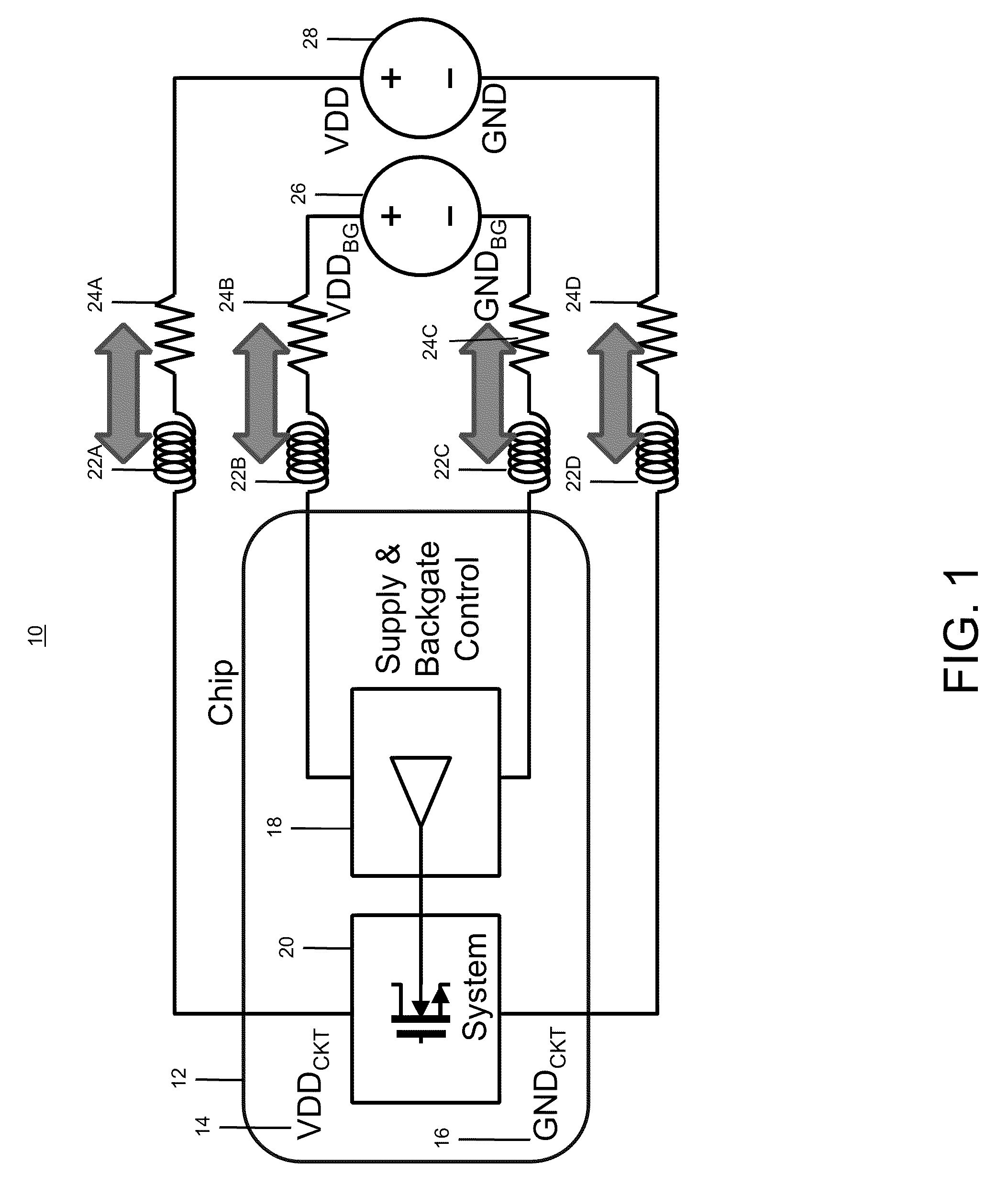
The present invention is about a circuit and method for quickly switching between sleep and normal modes for digital circuits. It uses chip internal charge transfer operations to put the circuit into fast sleep. This invention reduces external power involvement, and it expedites the sleep mode transition time by limiting charge transfers within the chip. The invention set forth herein uses high-level circuit block supports and is applicable to all circuits such as digital circuits. The fast sleep and fast wake-up enable a smarter power management of the system. This functionality also maximizes performance per power and provides a more energy efficient computing architecture. The circuit includes a supply voltage node, a ground voltage node, a set of backgate voltage nodes, and a charge transfer mechanism coupled to the supply voltage node, the ground voltage node, and the set of backgate voltage nodes. The charge transfer mechanism is configured to transfer charge among the supply voltage node, the ground voltage node, and the set of backgate voltage nodes. The method for changing modes of a digital circuit involves closing switches and transferring charge to put the circuit into sleep mode, and then opening the switches and transferring charge to bring the circuit out of sleep mode.

Problems solved by technology

Power conservation is a growing issue in circuitry as the recent trend towards more energy efficient data center design has become an important issue within Information Technology (IT) industry.
Specifically, a subsystem level stand-by (sleep mode) design has been available, but the current circuit design method does not allow for circuit level control of the stand-by operation.

Method used


Image

  • Internal charge transfer for circuits
  • Internal charge transfer for circuits
  • Internal charge transfer for circuits

Examples


Embodiment Construction

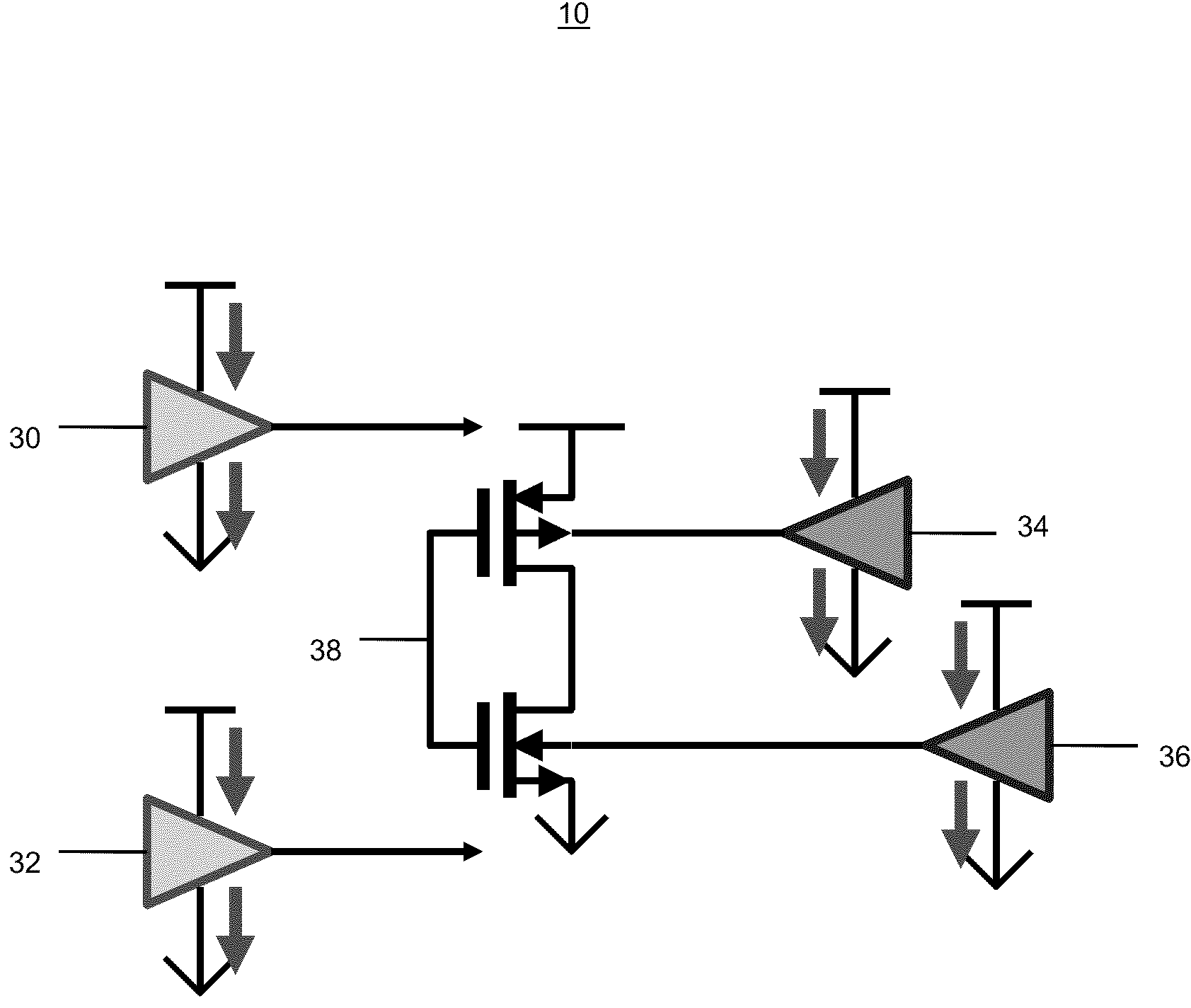
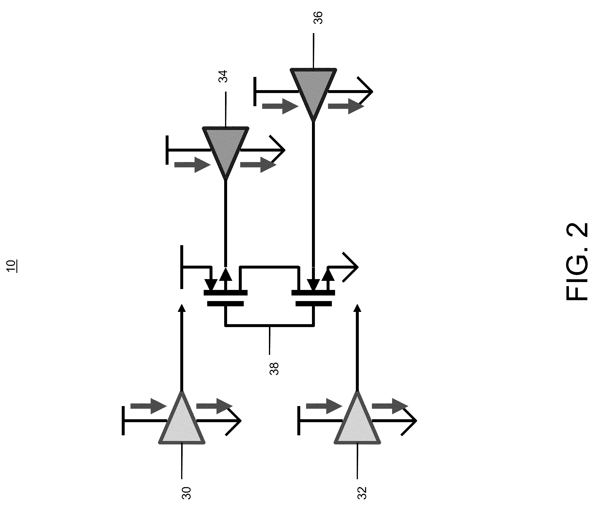
[0017]As indicated above (among other things) the present invention enables fast transition between sleep and normal modes for circuits such as digital circuits. This invention utilizes chip internal charge transfer operations to put the circuit into fast sleep. The invention reduces external power involvement, and it expedites the sleep mode transition time by limiting charge transfers within the chip. The invention set forth herein uses high-level circuit block supports and therefore it is applicable to all circuits such as digital circuits. The fast sleep and fast wake-up enable a smarter power management of the system. This functionality also maximizes performance per power, and provides a more energy efficient computing architecture. Among other things, a circuit in accordance with the present invention can include a supply voltage node, a ground voltage node; a set of backgate voltage nodes; and a charge transfer mechanism coupled to the supply voltage node, the ground voltage...


PUM


Abstract

The present invention enables fast transition between sleep and normal modes for circuits such as digital circuits. This invention utilizes chip internal charge transfer operations to put the circuit into fast sleep. The invention reduces external power involvement, and it expedites the sleep mode transition time by limiting charge transfers within the circuit. The fast sleep and fast wake-up enable more efficient power management of the system. This functionality also maximizes performance per power, and provides a more energy efficient computing architecture.

Description

CROSS-REFERENCE TO RELATED APPLICATIONS[0001]This application is related in some aspects to commonly owned and co-pending Ser. No. 12 / 275,508, entitled “Mounted Cache Memory in a Multi-Core Processor (MCP),” filed Nov. 21, 2008, the entire contents of which are herein incorporated by reference. This application is also related in some aspects to commonly owned and co-pending Ser No. 12 / 275,552, entitled “Cache Memory Sharing in a Multi-Core Processor (MCP),” filed Nov. 21, 2008, the entire contents of which are herein incorporated by reference. This application is also related in some aspects to commonly owned and co-pending Ser. No. 12 / 276,069, entitled “Pseudo Cache Memory in a Multi-Core Processor (MCP),” filed Nov. 21, 2008, the entire contents of which are herein incorporated by reference. This application is also related in some aspects to commonly owned and co-pending Ser. No. 12 / 276,072, entitled “Cache Memory Bypass in a Multi-Core Processor (MCP),” filed Nov. 21, 2008, the...

Claims


Application Information

Patent Timeline
Patent Type & Authority Patents(United States)
IPC IPC(8): H03K19/094
CPCH03K19/0016H03K19/00G11C19/28
Inventor CHO, CHOONGYEUNCORBIN, ELMER K.KIM, DAEIKKIM, MOON J.
Owner GLOBALFOUNDRIES US INC
Learn More