
Encapsulated leadframe semiconductor package for random access memory integrated circuits

a technology of random access memory and semiconductor packages, applied in semiconductor devices, semiconductor/solid-state device details, electrical apparatus, etc., can solve the problems of more advanced surface mount technology equipment, wire-bond interconnections exhibit a significant amount of inductance, and csp packages are more expensive to manufacture than

Active Publication Date: 2010-08-24
KINGSTON DIGITAL CO LTD
View PDF32 Cites 12 Cited by
  • Summary
  • Abstract
  • Description
  • Claims
  • Application Information

AI Technical Summary

Problems solved by technology

Hence, at high frequencies, such wire-bond interconnections exhibit a significant amount of inductance.
However, the CSP packages are more expensive to manufacture than TSOP packages and require more advanced surface mount technology equipment for board-level assembly and inspection.
Because of this limitation, new generations of SDRAMs having high system speeds are typically used in only the more expensive CSP packages.

Method used


Image

  • Encapsulated leadframe semiconductor package for random access memory integrated circuits
  • Encapsulated leadframe semiconductor package for random access memory integrated circuits
  • Encapsulated leadframe semiconductor package for random access memory integrated circuits

Examples


Embodiment Construction

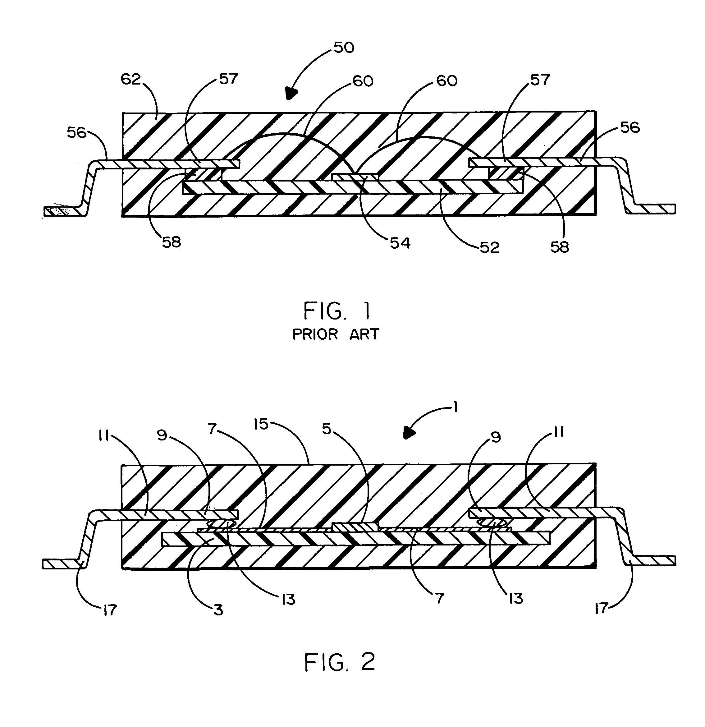
[0019]FIG. 1 of the drawings illustrates a conventional plastic leadframe semicondutor package 50 having a well known wire bond interconnect scheme. The semiconductor package 50 includes an integrated circuit (IC) device 52 having center bonding pads 54 (only one of which being shown) attached to the top surface thereof. The leadframe 56 is affixed to the top surface of IC device 52 by means of adhesive 58. The inner tips 57 of the leadframe 56 are electrically connected to the center bonding pads 54 by way of thin gold wires 60. The IC device 54, leadframe 56, and wire interconnects 60 are all encapsulated by a suitable molding (e.g. plastic) compound 62.

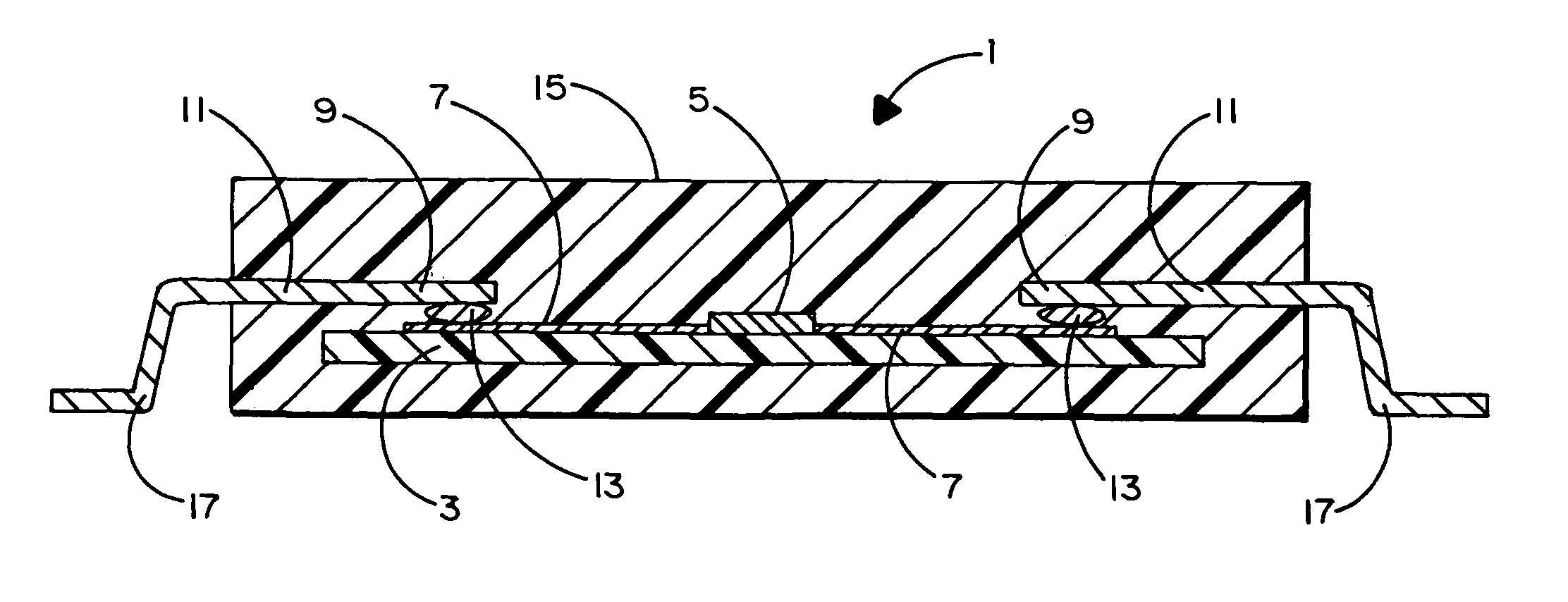
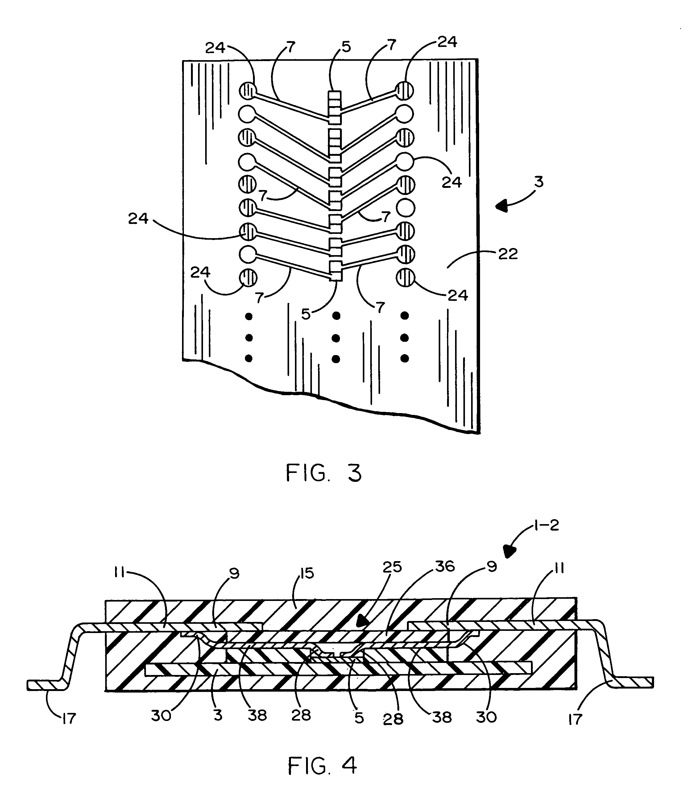
[0020]Referring to FIG. 2 of the drawings, the cross-section of a plastic leadframe semiconductor package 1 according to a first embodiment of this invention is shown having an IC device 3 with center input-output bonding pads 5 (only one of which is being shown). The center bonding pads 5 include conductive traces 7 to fan out the...


PUM


Abstract

A thin, small outline IC leadframe plastic package to be used to assemble high performance, high speed semiconductor memory IC devices such as dynamic random access memories (DRAM) having a high data transfer rate in the range of 1 GigaHertz. The package leadframe is electrically interconnected to the IC device input-output pads by either electrically conductive (e.g. solder) bumps that are flip-chip bonded to the IC device or by of an interposer. The interposer contains integral curled micro-spring contacts at opposite ends of conductive fan out traces. The interposer is attached to the leadframe bonding pads by way of tape automated bonding, soldering, or adhesive bonding. The leadframe that is interconnected to the IC device by the aforementioned flip-chip bumps or the interposer is encapsulated and trimmed to form either gull-wing style perimeter leads as a standard thin small outline package (TSOP) or wrap around leads as a micro-leadframe (MLF) package.

Description

BACKGROUND OF THE INVENTION[0001]1. Field of the Invention[0002]This invention relates to plastic leadframe semiconductor packages such as those used in the manufacture of dynamic random access memories (DRAM) that are capable of a high data transfer rate in the range of 1 GigaHertz.[0003]2. Background Art[0004]Dynamic random access memory (DRAM) integrated circuits are widely used in leadframe packages such as thin small outline packages (TSOP) for memory module assembly. TSOP packages have many advantages in the fabrication of dual inline memory modules (DIMM). These packages are characterized by a low (i.e. thin) profile, low manufacturing cost, relatively small size, and are generally compatible with common surface mount technology (SMT) equipment and processes. Accordingly, in recent years, TSOP packages have been the package of choice for use in most DIMM memory module assemblies.[0005]However, with the advent of high-speed and high-performance DRAM memory devices, the system ...

Claims


Application Information

Patent Timeline
Patent Type & Authority Patents(United States)
IPC IPC(8): H01L23/495H01L23/48
CPCH01L23/4951H01L23/49517H01L23/4952H01L23/49524H01L24/06H01L2224/0401H01L2224/04042H01L2224/06136H01L2224/16H01L2224/48091H01L2224/48247H01L2924/01013H01L2924/01029H01L2924/01042H01L2924/0105H01L2924/01079H01L2924/01082H01L2924/014H01L2924/30107H01L2924/00014H01L24/48H01L2924/01033H01L2924/01075H01L2924/01322H01L2224/45144H01L2924/00H01L2224/16245H01L2224/32245H01L2224/73215H01L2224/45015H01L2924/15787H01L2924/181H01L24/45H01L2224/4826H01L2924/14H01L2924/00015H01L2224/05599H01L2924/00012
Inventor KOH, WEI H.KONG, FREDCHEN, DAVID
Owner KINGSTON DIGITAL CO LTD
Learn More