Eureka AIR delivers breakthrough ideas for toughest innovation challenges, trusted by R&D personnel around the world.

Quantum-imaging system and mode of operation and method of fabrication thereof

a quantum imaging and quantum-imaging technology, applied in the field of radiation detection, can solve the problems of high noise and cross-talk effect, over-complexity, and inability to operate at cryogenic temperatures, and achieve high selectivity, high energy resolution of isotopic lines, and high precision of relative photon flux measurement

Active Publication Date: 2010-08-24
MERCURY MISSION SYST LLC
View PDF3 Cites 18 Cited by
  • Summary
  • Abstract
  • Description
  • Claims
  • Application Information

AI Technical Summary

Benefits of technology

[0044]In contrast to conventional electronic-readout devices, a quantum-imaging device can be provided that incorporates an optical readout. Accordingly, such a device can be implemented without including the complex pixel / electrode structure that is attached to the crystal in conventional devices. Additionally, in one embodiment the crystal does not need to be CdTe or CZT, and can be made from a variety of birefringent materials including, for example, BGO or BSO, which can be large and still preserve high quality; thus preserving high capture rate, as well as high reliability and repeatability. Accordingly, some embodiments can be attractive for mass production and operation in harsh outdoor conditions. Additionally, in other embodiments, this quantum-imaging device can be configured to operate as both a photon counter and a photon spectrometer.
[0045]Embodiments of the quantum-imaging device can be implemented to provide identification of isotopic lines by measurement of both photon fluxes and photon energies. Photon fluxes can be measured for both strong and weak photon beams. In one embodiment, weak photon beams can be measured down to approximately 1 pJ / cm2sec, or 0.1 pSv / h-level. Preferably, the device can be implemented such that photon energies can be measured with high resolution such as, for example, 1% or better, within an energy range of approximately 10 keV to 1.2 MeV. An important advantage that can be obtained by the quantum-imaging system in various embodiments is that it can be implemented to perform as both a γ-counter and a γ-spectrometer, working in room temperature, and in harsh outdoor conditions.
[0052]The disclosed quantum-imaging technology can be implemented in one or more various embodiments that can be configured to provide one or more of the below described benefits over current approaches. For example, the quantum-imaging technology might be implemented to include one or more of the following features such as: The ability to work both as a γ-counter and a γ-spectrometer; a structure that can provide imaging and does not use the complex pixel / electrode structure needed for electronic read-out; a BSO or BGO crystal (or other birefringent material) detection device that can be large, while still preserving high quality, thereby maintaining high photon capture rate by photo-absorption—a feature that is important for high device sensitivity. As other examples, in various embodiments the quantum-imaging technology might also be implemented to provide a quantum-imaging system that operates both at room temperature and in harsh outdoor conditions; that has high mechanical stability (for example, because the complex pixel / electrode structure can be avoided); that can provide easy (x,y,z)-volume readout (for example, with embodiments implementing a multi-layer architecture as described below); that has high energy resolution (˜1%) across a broad energy spectrum (not only for high energy photons, >500 keV); that can work for a large number (˜10) of isotopic lines, in parallel; and is easy to fabricate and provides ease of maintenance and operation with cost-effective components and technologies.
[0055]Preferably, the quantum-imaging system can be configured in various embodiments to incorporate highly innovative quantum-imaging techniques based on the visualization of a secondary electron cloud generated by an impinging photon. This feature can be implemented to provide high selectivity. For example, embodiments can be implemented to achieve high energy resolution of isotopic lines or highly precise measurement of relative photon fluxes. This can allow the device to accomplish highly selective identification of isotopic γ-sources.
[0056]In another embodiment, a variable absorption path method can be utilized to allow for double checking of photon energy. In yet another embodiment, a multi-layer architecture can be provided. For example, the elimination of the pixel / electrode structure can allow for realization of a multilayer architecture, which can be utilized in various embodiments to detect high energy photons, for example, with energies from approximately 200 keV to 3 MeV, and higher. A multilayer architecture can also allow for both (x,y,z)-photon imaging, and for selectively reducing photon fluxes to avoid or reduce overlap of secondary electron clouds. The use of the several innovative optical read-out techniques can also be provided, some of which are based on or derived from conventional imaging technologies.

Problems solved by technology

However, these only operate at cryogenic temperatures.
This electrode structure, however, is fragile and suffers from significant noise and cross-talk effects.
These detectors with such an electrode arrangement do provide electron cloud visualization, but instead rely on the complex electronic structure, which is overly complex and fragile.
In addition, the CdTe / CZT-crystals typically should be rather small to achieve high quality measurements, which compromises photon capture rate defined by photo-absorption.
Therefore, the electronic read-out spectrometers based on high energy gap semiconductors such as CdTe or CZT (to operate in room temperature) have quality, reliability, and repeatability problems, which makes production problematic, especially for harsh outdoor conditions.
Unfortunately, there are several disadvantages in current experimental units based on these crystals.
Such disadvantages include the transmission mode of operation, a scanning approach using a single photomultiplier tube (PMT) for detection, and high-intensity scanning He—Ne laser beam with low polarization contrast for readout.
Perhaps the most serious drawback is the inability of thin 50 um crystals (necessary for reasonable resolution) to provide high capture volume for absorption of hard X-rays and γ photons (energies >100 keV).
Accordingly, such systems are unpractical for photon counting or photon spectrometry.
Additionally, conventional Pockel cells arrangements with optical beam technologies suffer from a variety of shortcomings.
The inventors have discovered that this natural and obvious arrangement employed in conventional systems, which leads to a square dependence of the signal on the charge density n(x,y) is problematic because the signal for electrons produced by high-energy photons practically vanishes, and the nonlinearity complicates the charge integration, especially for secondary electron clouds of small sizes.
This complicated detector is capable only for detecting radiation fluxes, and it has low sensitivity.
It does not allow secondary electron cloud visualization, photon counting or photon spectrometry.

Method used


Image

  • Quantum-imaging system and mode of operation and method of fabrication thereof
  • Quantum-imaging system and mode of operation and method of fabrication thereof
  • Quantum-imaging system and mode of operation and method of fabrication thereof

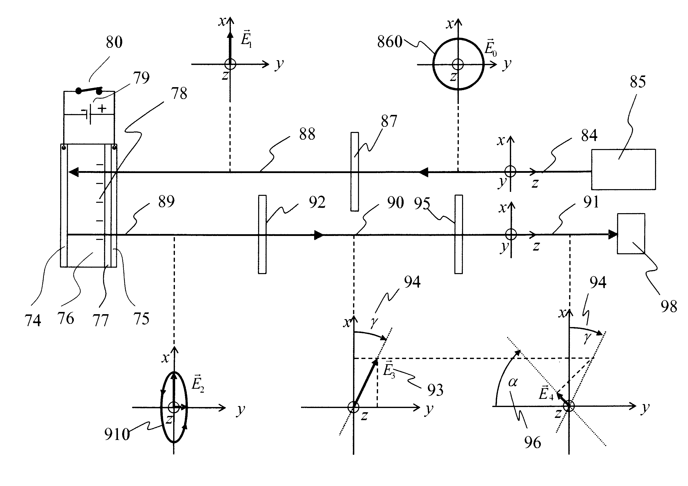
Examples

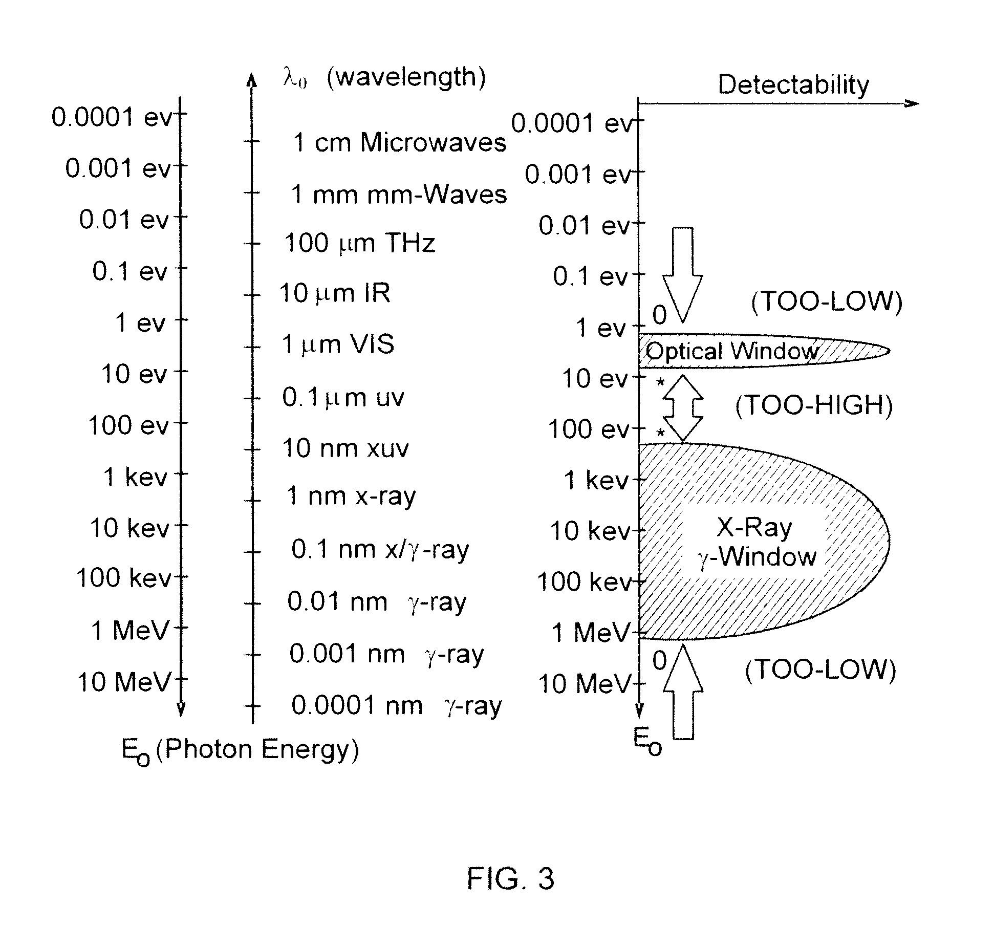

Embodiment Construction

[0041]According to various embodiments of the invention, a quantum-imaging system for detecting photons, including short-wavelength (2) for both strong beams and weak beams, the latter ones in the intensity range of 1 pJ / cm2·sec, or 0.1 μSv / h. The quantum-imaging system can also function as a photon spectrometer because it can measure photon energies with high energy resolution such as, for example, 1% of photon energy.

[0042]The quantum-imaging system can be configured as an optical read-out system that measures secondary electron clouds generated by a primary photon, transferred into a spatial pattern. In one embodiment, the spatial pattern formed by the secondary electron cloud is read and transmitted by an optical read-out beam. In contrast to electronic-readout systems, which require complex pixel / electrode structure to measure photon energy, a quantum-imaging system using an optical read-out can be configured to measure short-wavelength photons while avoiding this complex pixel...


PUM


Abstract

A quantum-imaging system for detecting photons, including short-wavelength (<1 nm) photons, is provided. A quantum imaging system can include optical read-out and optical means, and can be configured to perform as both a photon counter and a photon spectrometer. A quantum-imaging system can function as a photon counter and be configured to measure photon beam fluences (e.g., in J / cm2) for both strong beams and weak beams, the latter ones, for example, in the intensity range of 1 pJ / cm2sec, or 0.1 μSv / h. The quantum-imaging system can also function as a photon spectrometer and can be configured to measure photon energies with high energy resolution such as, for example, 1% of photon energy.

Description

RELATED APPLICATION[0001]This application is a continuation of and claims the benefit of U.S. patent application Ser. No. 12 / 046,976, entitled “Quantum-Imaging System and Mode of Operation and Method of Fabrication Thereof,” filed Mar. 12, 2008 now abandoned, which is incorporated herein by reference.TECHNICAL FIELD[0002]The present invention relates to radiation detection, and more particularly, some embodiments relate to measurement of photon fluxes and photon energy for short-wavelength photons (<1 nm), employing an optical read-out configured to provide visualization of secondary electron clouds generated by those photons.DESCRIPTION OF THE RELATED ART[0003]Many medical, security, and military applications require the capability to measure photon energy in room-temperature environments (or with modest cooling), and photon fluxes for short-wavelength photons (<1 nm). Some applications require that the measurement be obtained from isotopic lines generated by radioactive isot...

Claims


Application Information

Patent Timeline
Patent Type & Authority Patents(United States)
IPC IPC(8): G01T1/185
CPCG01T1/29
Inventor JANNSON, TOMASZPRADHAN, RANJITGERTSENSHTEYN, MICHAELGRUBSKY, VICTORMARIENKO, IGORMEDVEDKIN, GENNADYMENGESHA, WONDWOSENROMANOV, VOLODYMYRYANG, YUNPING
Owner MERCURY MISSION SYST LLC
Why Eureka
Eureka Blog
Learn More