
Optical element damping systems

a technology of optical elements and damping systems, applied in the field of lithography, can solve problems such as the motion of optical elements, and achieve the effect of increasing damping

Active Publication Date: 2010-07-06
ASML HLDG NV
View PDF8 Cites 4 Cited by
  • Summary
  • Abstract
  • Description
  • Claims
  • Application Information

AI Technical Summary

Benefits of technology

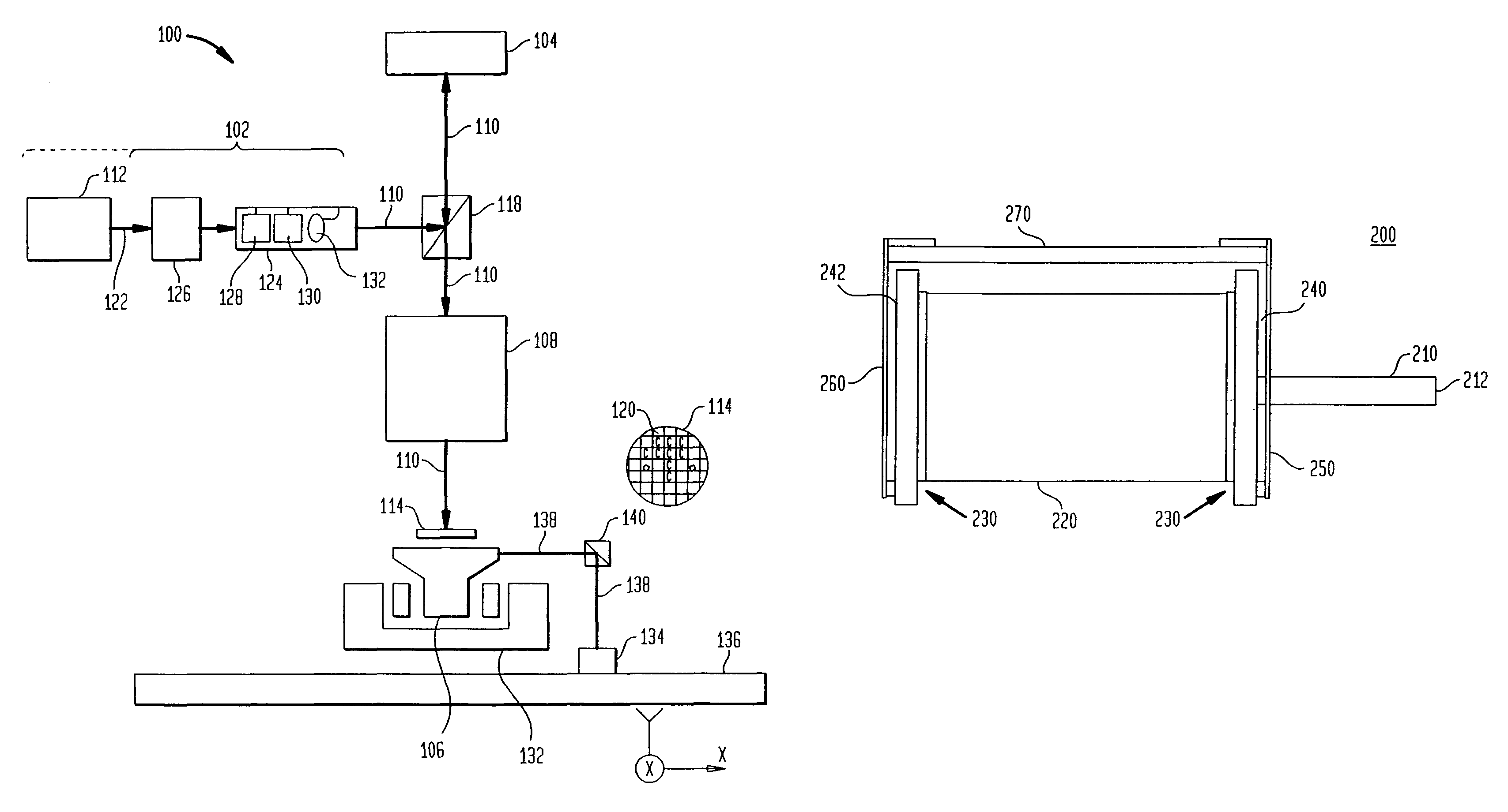
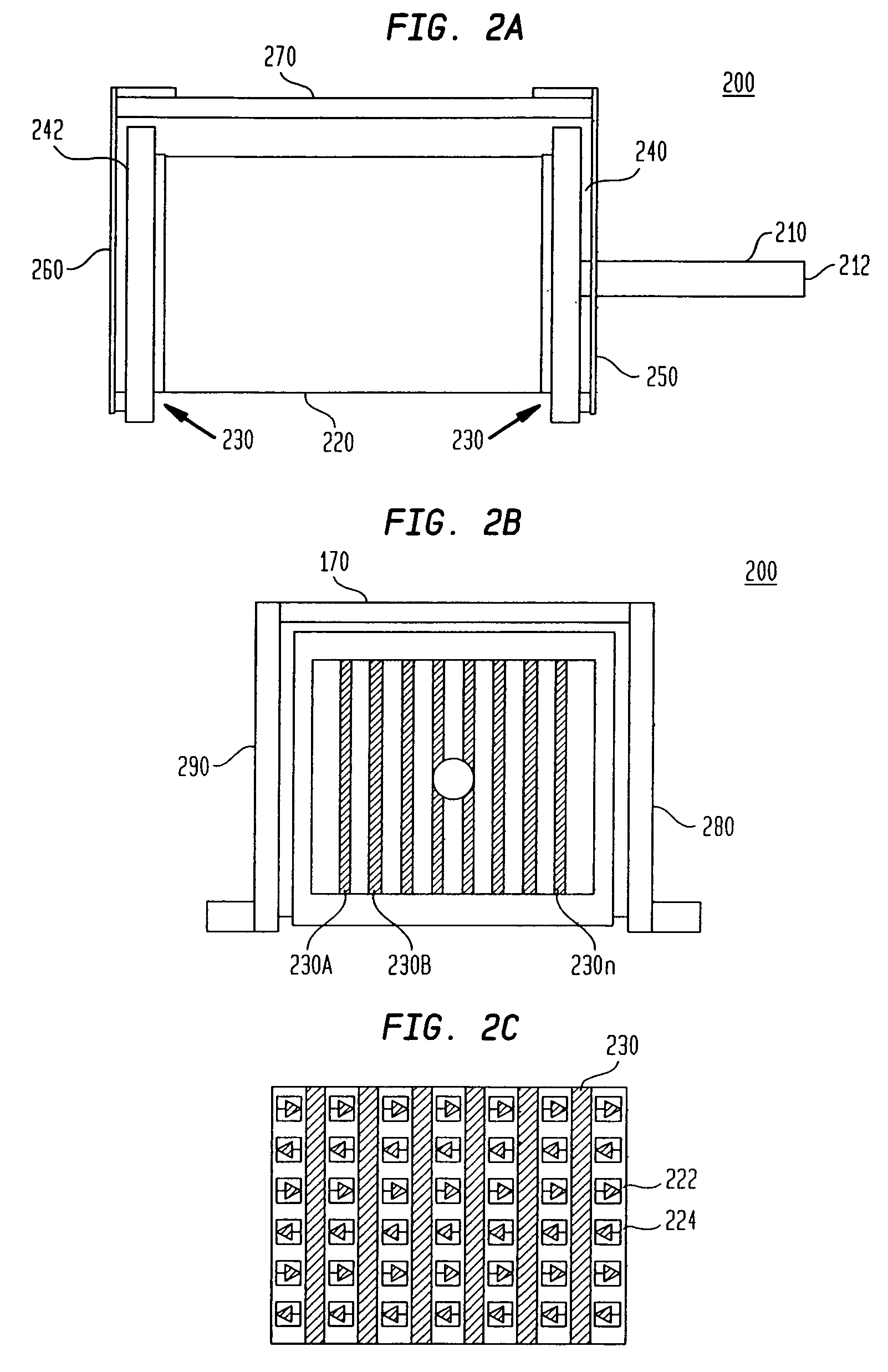
[0019]The present invention is directed to optical element damping systems. In particular, an eddy current damper is disclosed. The eddy current damper includes a rod, a series of conducting plates coupled to the rod, and alternating layers of magnets. The alternating layers have alternating magnetic fields. When an optical element moves, the optical element will exert a force on the rod. The rod causes the conducting plates to move relative to the alternating layers of magnets to generate eddy currents within each of the conducting plates, such that the eddy currents damp the motion of an optical element. In an alternative embodiment, a motion amplifier is used to provide additional mechanical advantage that significantly increases the damping provided by the eddy current damper for a given damper volume.
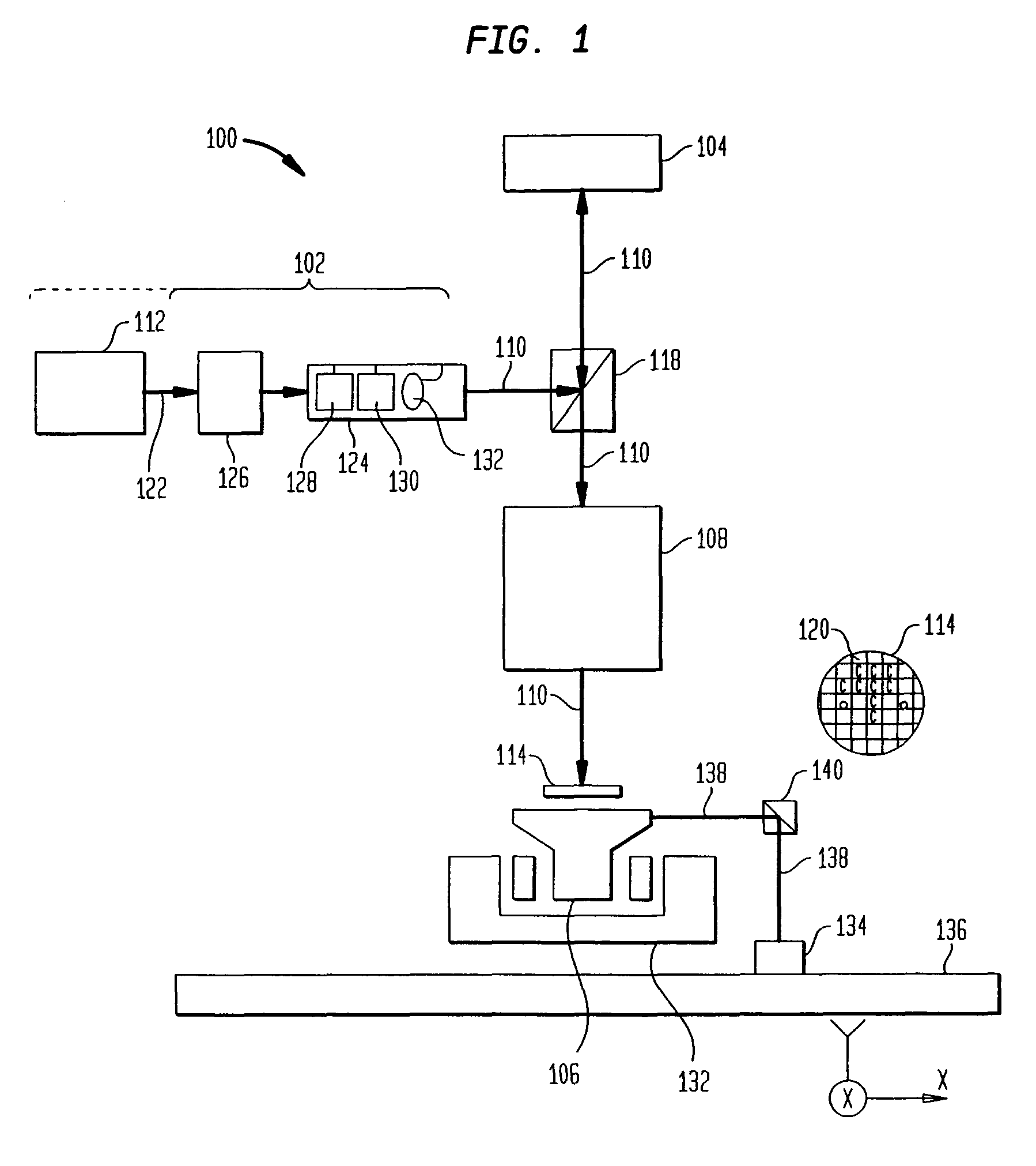
[0021]In still further aspects of the invention, eddy current dampers are provided within conventional scanning lithography devices and optical maskless lithography devices to improve performance by stabilizing optical element motion.
[0022]The present invention provides numerous benefits. First the present invention improves overlay performance for optical maskless lithography systems. Second, the present invention reduces image smearing performance for conventional lithographic scanner systems. Third, improved overlay performance for traditional lithographic stepper systems is achieved. In general, the present invention tolerates acoustic and base vibration in lithographic systems, while avoiding over constraining the lens optical and opto-mechanical designs.

Problems solved by technology

The rod causes the conducting plates to move relative to the alternating layers of magnets to generate eddy currents within each of the conducting plates, such that the eddy currents damp the motion of an optical element.

Method used


Image

  • Optical element damping systems
  • Optical element damping systems
  • Optical element damping systems

Examples


Embodiment Construction

[0037]While the present invention is described herein with reference to illustrative embodiments for particular applications, it should be understood that the invention is not limited thereto. Those skilled in the art with access to the teachings provided herein will recognize additional modifications, applications, and embodiments within the scope thereof and additional fields in which the invention would be of significant utility.

[0038]Although specific reference may be made in this text to the use of lithographic apparatus in the manufacture of integrated circuits (ICs), it should be understood that the lithographic apparatus and projection systems described herein may have other applications, such as, for example, the manufacture of DNA chips, MEMS, MOEMS, integrated optical systems, guidance and detection patterns for magnetic domain memories, flat panel displays, thin film magnetic heads, etc. The skilled artisan will appreciate that, in the context of such alternative applica...


PUM


Abstract

The present invention is directed to optical element damping systems. In particular, an eddy current damper is disclosed. The eddy current damper includes a rod, a series of conducting plates coupled to the rod, and layers of magnets. The alternating layers have alternating magnetic fields. When an optical element moves, the optical element will exert a force on the rod. The rod causes the conducting plates to move relative to the alternating layers of magnets to generate eddy currents within each of the conducting plates, such that the eddy currents damp the motion of an optical element. In an alternative embodiment, an eddy current damper motion amplifier is used to provide additional mechanical advantage that significantly increases the damping provided by the eddy current damper. Eddy current dampers are provided within conventional scanning lithography devices and optical maskless lithography devices to improve performance by stabilizing optical element motion.

Description

CROSS REFERENCES TO RELATED APPLICATIONS[0001]This application claims the benefit of priority to U.S. Provisional Patent Application, Application No. 60 / 754,898, filed Dec. 30, 2005, which is incorporated herein by reference in its entirety.BACKGROUND OF THE INVENTION[0002]1. Field of the Invention[0003]The present invention relates to lithography, and more particularly, to optical element damping systems.[0004]2. Background of Invention[0005]Lithography is a process used to create features on the surface of substrates. Such substrates can include those used in the manufacture of flat panel displays (e.g., liquid crystal displays), circuit boards, various integrated circuits, and the like. A frequently used substrate for such applications is a semiconductor wafer or glass substrate.[0006]During lithography, a wafer, which is disposed on a wafer stage, is exposed to an image projected onto the surface of the wafer by exposure optics located within a lithography apparatus. While expos...

Claims


Application Information

Patent Timeline
Patent Type & Authority Patents(United States)
IPC IPC(8): G02B7/02
CPCG02B7/00G03F7/70825G03F7/709
Inventor ROUX, STEPHENKOCHERSPERGER, PETERKREUZER, JUSTIN
Owner ASML HLDG NV
Learn More