
Test vector generating method and test vector generating program of semiconductor logic circuit device

a technology of logic circuit device and test vector, which is applied in the direction of instruments, error detection/correction, computing, etc., can solve the problems of power consumption remarkably larger in a test mode than in a usual operation mode, and the controllability of pseudo external input lines and observability of pseudo external output lines, so as to avoid an erroneous test, reduce power supply voltage, and reduce power consumption

Inactive Publication Date: 2010-06-22
LPTEX
View PDF18 Cites 10 Cited by
  • Summary
  • Abstract
  • Description
  • Claims
  • Application Information

AI Technical Summary

Benefits of technology

"The present invention provides a method for generating test vectors for a semiconductor logic circuit device that reduces the number of output switching scan flip-flops in a double-capture operation, thus decreasing double-capture power consumption and avoiding erroneous tests. The method involves forming a combinational portion and a scan flip-flop group connected between external input and output lines. The combinational portion is hypothetically formed by first and second combinational portions with common external input lines. The scan flip-flop group is hypothetically formed by first and second scan flip-flops operated by first and second capture clock pulses. A first filling step fills X-bits of a test cube to decrease the number of discrepancies between bits of the external input and output lines. A second filling step repeats the first filling step to decrease the number of discrepancies between bits of the external input lines of the first combinational portion and the external output lines of the second combinational portion. A balancedly discrepancy decreasing step repeats the first and second filling steps to decrease the number of discrepancies between bits of the external input lines of the first combinational portion and the external output lines of the second combinational portion in a balanced manner. A third filling step fills all specified bits of the external input lines when there is no X-bit in the pseudo external input lines, the pseudo external output lines, and the pseudo external input lines of the second combinational portion. The test vector generated using this method has no X-bits and reduces power consumption."

Problems solved by technology

However, it is generally impossible to directly access the output lines of the flip-flops (the pseudo external input lines) and the input lines of the flip-flops (the pseudo external output lines) in the semiconductor logic circuit device from the exterior.
Therefore, in order to test the combinational portion, there are problems in the controllability of the pseudo external input lines and the observability of the pseudo external output lines.
Despite the effectiveness of the above-mentioned real speed scan test system, there is a problem in that the power consumption is remarkably larger in a test mode than in a usual operation mode.
For example, if the semiconductor logic circuit device is constructed by CMOS circuits, the power consumption consists of static power consumption due to leakage currents and dynamic power consumption due to switching operations of the logic gates and the flip-flops.
Additionally, the latter dynamic power consumption consists of shift power consumption in shift operations and capture power consumption in capture operations.
As a result, the shift power consumption is increased to induce excessive heat.
Therefore, semiconductor logic circuit devices would be damaged.
The IR drop phenomenon would erroneously operate the circuit resulting in erroneous test response values in the scan flip-flop group 12.
Thus, even semiconductor logic circuit devices normally operable in a usual state would be deemed to be defective in a test state, which can be an erroneous test.
As a result, the manufacturing yield would be decreased.
Particularly, when semiconductor logic circuit devices become ultra-large in scale, more fine-structured and lower in power supply voltage, the manufacturing yield caused by the erroneous test would be remarkably decreased.
The capture power consumption can be decreased by a clock gating technique; however, this would remarkably affect the physical design of semiconductor logic circuit devices.
Also, the capture power consumption can be decreased by a one hot technique or a multiple clock technique; however, the former technique would remarkably increase test data amount, and the latter technique would require enormous memory consumption in generating test vectors, which is a shortcoming.

Method used


Image

  • Test vector generating method and test vector generating program of semiconductor logic circuit device
  • Test vector generating method and test vector generating program of semiconductor logic circuit device
  • Test vector generating method and test vector generating program of semiconductor logic circuit device

Examples


Embodiment Construction

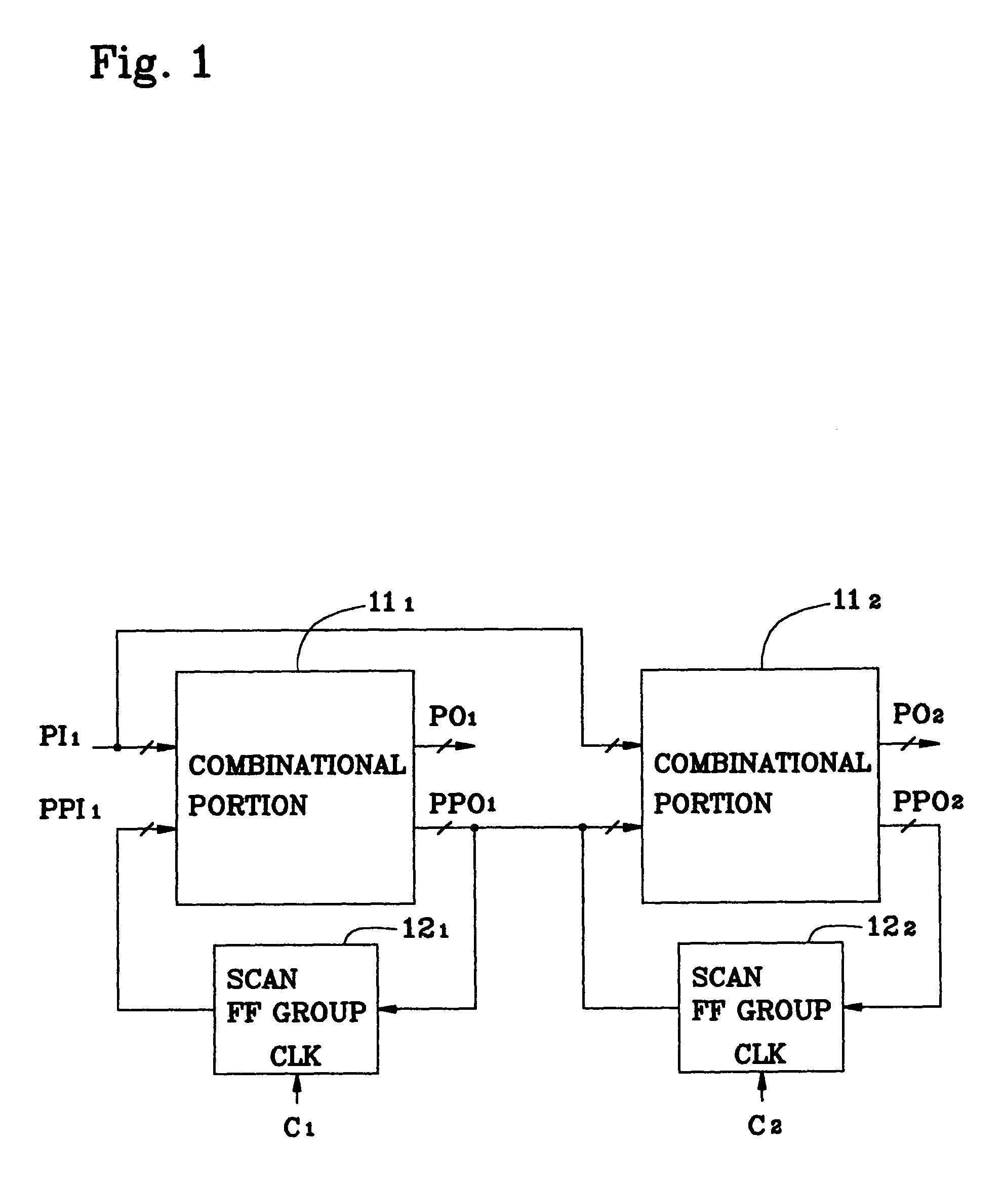
[0031]FIG. 1 is a circuit expansion view showing the principle of a test vector generation of a semiconductor logic circuit device according to the present invention.

[0032]FIG. 1 is used for explaining the reduction of the power consumption in the case where the semiconductor logic circuit device of FIG. 14 is subjected to double-capture pulses C1 and C2. Therefore, the combinational portion 11 and the scan flip-flop groups 12 of FIG. 14 are hypothetically doubled, i.e., combinational portions 111 and 112 each being the same as the combinational portion 11 and scan flip-flop groups 121 and 122 each being the same as the scan flip-flop group 12 are hypothetically doubled. In this case, external input lines PI1 of the combinational portion 111 serve as external input lines PI2 of the combinational portion 112, and pseudo external output lines PPO1 of the combinational portion 111 serve as pseudo external input lines of the combinational portion 112. Further, the scan flip-flop group 1...


PUM


Abstract

The X-type of each bit permutation is determined (step 301). When there are X-types except for X-type 1, i.e., X-type with no don't-care bits, total capture state transition numbers TECTA1 and TECTA2 for capture clock pulses C1 and C2 are calculated (step 303). As a result, when TECTA1>TECTA2, an X-type is selected for the capture clock pulse C1 and a first X-filling processing is performed (see step 305). On the other hand, when TECTA1≦TECTA2, an X-type is selected for the capture clock pulse C2 and a second X-filling processing is performed (step 306).

Description

TECHNICAL FIELD[0001]The present invention relates to a test vector generating method and test vector generating program of a semiconductor logic circuit device for carrying out a real-speed scan test targeting a delay fault.BACKGROUND TECHNOLOGY[0002]Semiconductor logic circuit devices are shipped through three steps, i.e., a design step, a production step and a test step. In a test step, a test vector is applied to a manufactured semiconductor logic circuit device, to observe a test response from the semiconductor logic circuit device, and to compare the test response with an expected test response, thus determining whether the semiconductor logic circuit device is good or defective. The rate of good semiconductor logic circuit devices is called a manufacturing yield which would remarkably affect the semiconductor logic circuit devices in manufacturing cost.[0003]Generally, a semiconductor logic circuit device (mainly, a sequential circuit) is constructed by a combinational portio...

Claims


Application Information

Patent Timeline
Patent Type & Authority Patents(United States)
IPC IPC(8): G06F11/00
CPCG01R31/318547G01R31/3183G01R31/28
Inventor WEN, XIAOQINGKAJIHARA, SEIJI
Owner LPTEX
Learn More