Near infrared twin photon source

Inactive Publication Date: 2010-06-01
ECOLE POLYTECHNIQUE FEDERALE DE LAUSANNE (EPFL)
View PDF1 Cites 9 Cited by
  • Summary
  • Abstract
  • Description
  • Claims
  • Application Information

AI Technical Summary

Benefits of technology

[0004]It is the object of the present invention to provide an optical parametric oscillator and a corresponding method of providing optical parametric oscillations that are easy to realize and that include signal and idler modes of comparable signal intensities.
[0016]Contrary to the embodiment as described above, a localization of polaritons in a microcavity structure could also be achieved by reducing the lateral dimensions of a microcavity, e.g. by an etching process, and without locally changing the cavity length. However, due to the interaction of the excitonic part of the polariton with the outside environment of the microcavity (e.g. the surrounding air) polaritons in such a structure would exhibit a reduced lifetime which in turn results in broadened linewidths of the polaritons and thus an overlap and disappearance of the quantized levels.
[0020]The microcavity as well as the layer including a raised or recessed region is preferably produced with semiconductor growth and lithographic processing techniques such as molecular beam epitaxy (MBE) or metal organic chemical vapors deposition (MOCVD) or others. Suitable materials for the microcavity include III-V semiconductors such as GaAs and AlGaAs. This permits an easy fabrication of devices including slight local variations of the cavity length. For example, an optical parametric oscillator working in the near infrared requires a cavity comprising a length in the order of a few microns. In such a cavity variations of the cavity length of a few nanometers are sufficient to obtain a significant localization effect.
[0027]According to one embodiment the method can include a step of forming said microcavity with at least one region having a different cavity length than a portion of said microcavity surrounding said region. Due to the local change of the length of the cavity a polariton can be localized without reducing or negatively influencing its lifetime and the spectral linewidth of its photonic part. The depth of the “potential trap” for the polaritons is directly defined by the change of the length of the cavity.

Problems solved by technology

Furthermore, in OPOs of this conventional type signal and idler photonic emissions comprise strongly unequal intensities.

Method used


Image

  • Near infrared twin photon source
  • Near infrared twin photon source
  • Near infrared twin photon source

Examples


Embodiment Construction

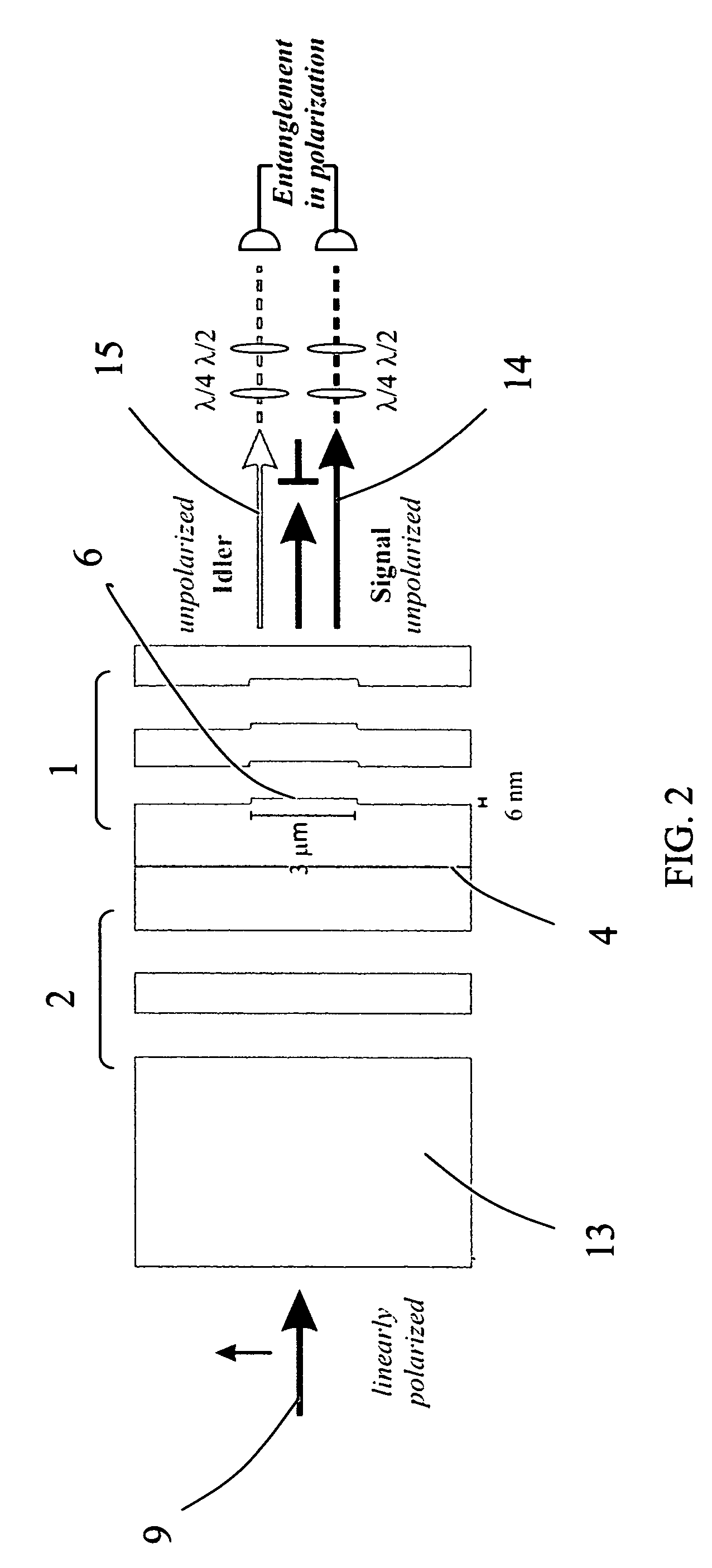
[0037]An optical parametric oscillator structure according to one embodiment of the invention is shown in FIG. 1. It includes a microcavity comprising two Bragg reflectors 1, 2 formed of alternating layers of GaAs and AlAs. The Bragg reflectors 1, 2 are separated by two semiconductor layers 3 of GaAs that surround a single quantum well 4 of In0.04Ga0.96As. Its fundamental energy level corresponds to a wavelength of 835 nm. The quantum well is slightly doped (14%) with In which allows to excite the microcavity through the GaAs substrate and to collect the light in transmission.

[0038]The distance between the Bragg reflectors corresponds to the wavelength of the fundamental quantum well level. Thus, the formation of a polariton, i.e. the superposition of a photon and an exciton in the strong coupling regime is granted. The semiconductor layers are sequentially grown on a substrate13 using molecular beam epitaxy (MBE). For the purpose of illustration only a reduced number of the semicon...


PUM

PropertyMeasurementUnit
heightaaaaaaaaaa
heightaaaaaaaaaa
lengthaaaaaaaaaa

Abstract

Optical parametric oscillator including a semiconductor microcavity being configured to spatially localize polaritons of at least three quantized polariton energy levels to effect an optical parametric oscillation.

Description

FIELD OF INVENTION[0001]The invention relates to a new optical semiconductor device and in particular to a micro optical parametric oscillator.BACKGROUND[0002]Optical parametric oscillators (OPOs) are frequently used as tunable infrared light sources. Conventionally they are realized by an optically pumped laser cavity including a non-linear crystal. The parametric oscillation is effected by irradiating the nonlinear crystal with an intense pump beam having a frequency ν3. In the nonlinear crystal quantum correlated photons of frequencies ν1 and ν2 are generated spontaneously by parametric scattering according to the relation ν3=ν1+ν2, wherein ν1 is the photon frequency. The generated modes are denoted as signal and idler modes.[0003]Conventional OPOs usually require a lengthy and inconvenient initial alignment procedure and during their operation a continuous feedback control of the cavity length in order to compensate for cavity length fluctuations. Furthermore, in OPOs of this co...

Claims


Application Information

Patent Timeline
Patent Type & Authority Patents(United States)
IPC IPC(8): G02F1/35G02F2/02
CPCB82Y20/00G02F1/39G02F2001/3509G02F2201/17G02F2201/346H01S5/18358G02F2202/108G02F2202/36G02F2203/15H01S5/18327G02F2202/101G02F1/3509
Inventor EL DAIF, OUNSIBAAS, AUGUSTINDEVEAUD-PLEDRAN, BENO TMORIER-GENOUD, FRANCOIS
Owner ECOLE POLYTECHNIQUE FEDERALE DE LAUSANNE (EPFL)
Why Eureka
Try Eureka