System package using flexible optical and electrical wiring and signal processing method thereof

a technology of flexible optical and electrical wiring and system package, which is applied in the direction of optical elements, instruments, semiconductor/solid-state device details, etc., can solve the problems of device not fully functioning as system package, processing and transmitting data errors become possible, etc., to prevent electronic process malfunction, easy to bend, and easy to install

Active Publication Date: 2010-05-18
KOREA PHOTONICS TECH INST
View PDF7 Cites 10 Cited by
  • Summary
  • Abstract
  • Description
  • Claims
  • Application Information

AI Technical Summary

Benefits of technology

[0011]In order to solve the above described problems in the related art, a system package using flexible opto-electric connections is provided, which can solve thermal problems by providing spacing between rigid substrates using a flexible substrate and can minimize electromagnetic wave interference that occurs when connecting high-speed data signals, by using the optical waveguides in the flexible substrate to effectively transmit data.
[0018]Since the system package is formed by connecting the plurality of rigid substrates using the flexible substrate that can be easily bent, it can be changed into various structures and easily installed without any structural limitation.
[0019]Also, as the rigid substrates are electrically and optically connected by including opto-electric wiring (optical waveguides and electrical wiring) inside the flexible substrate, high-speed signal transmission can be achieved. Also, as the rigid substrates are formed by being spaced by a predetermined distance from each other, thermal problems caused by the integrated circuits is solved, which prevents the malfunction of the electronic processes.
[0020]Further, as the signals are transmitted through the opto-electric wiring inside of the flexible substrate, the electromagnetic wave interference problem caused due to the signal speed and the wire length is solved, such that errors in transmitting signals are prevented.

Problems solved by technology

However, as various devices become more highly integrated, electromagnetic interference and thermal problems occur between the devices, such that errors in processing and transmitting data become possible.
As a result, there occurs a disadvantage in that the devices do not fully function as the system package.

Method used


Image

  • System package using flexible optical and electrical wiring and signal processing method thereof
  • System package using flexible optical and electrical wiring and signal processing method thereof
  • System package using flexible optical and electrical wiring and signal processing method thereof

Examples


Embodiment Construction

[0032]Reference will now be made in detail to the embodiments of the present invention, examples of which are illustrated in the accompanying drawings.

[0033]A system package can be used by integrating a system on package (SOP), a system in package (SIP), and a multi-chip module (MCM).

[0034]Hereinafter, the various embodiments of the present invention will be described in detail with reference to the accompanying drawings. When inserting reference numerals into the constituents in the respective drawings, although the constituents are illustrated in different drawings, so far as the constituents are the same, they are described to have the same reference numeral, where possible. The detailed description for the well-known function and constitution, judged to make the gist of the invention obscure, will be omitted.

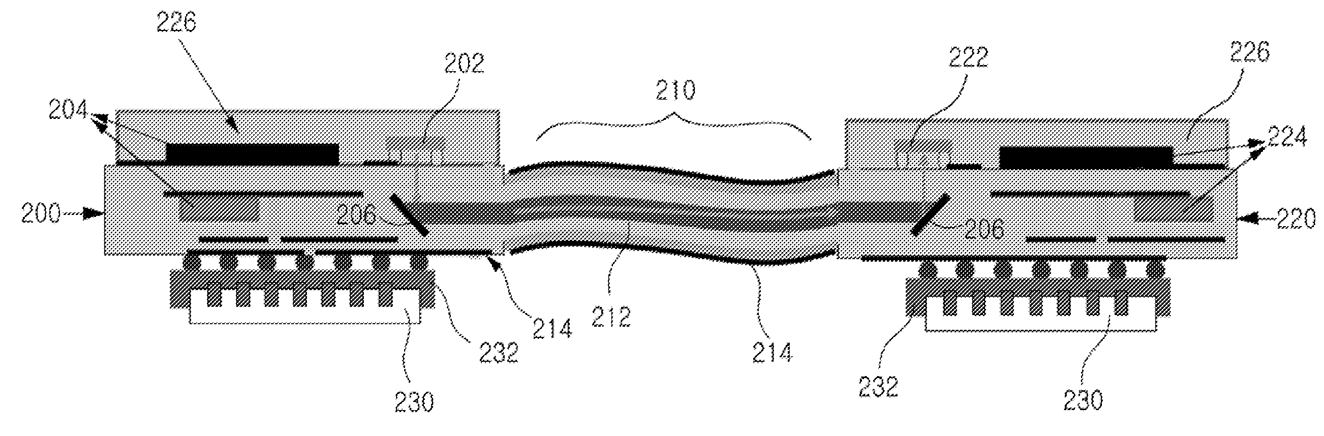
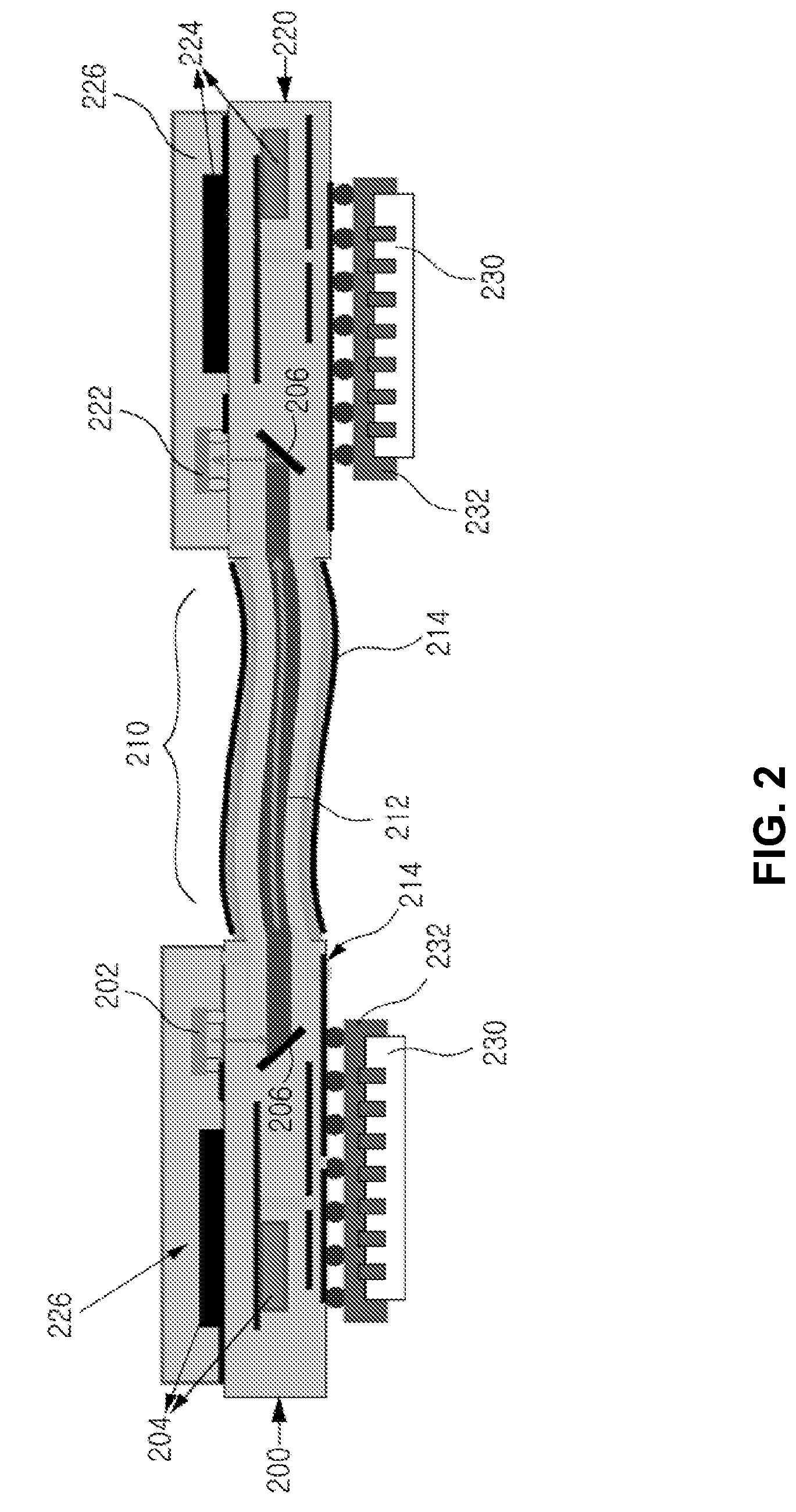
[0035]FIG. 2 is a cross-sectional view showing a system package using flexible opto-electric wiring according to one embodiment of the present invention. The system package ...


PUM


Abstract

A system package using flexible optical waveguides and electrical wires, and a signal processing method thereof are disclosed. Several rigid substrates having highly integrated electronic elements and optical elements mounted thereon can be electrically and optically connected by using flexible substrates that are electrically wired and optically connected. The package can be variously changed when configuring the package by the flexible substrate and the heat dissipation device and the electromagnetic shielding device are installed in the inside of the package, making it possible to solve electromagnetic wave interference problems and thermal problems occurring in the inside of the package.

Description

CROSS-REFERENCE TO RELATED APPLICATIONS[0001]This application claims priority to Korean Patent Application No. 10-2008-0003925, filed on Jan. 14, 2008, the entire contents of which is hereby incorporated by reference.BACKGROUND OF THE INVENTION[0002]1. Field of the Invention[0003]The present invention relates to a system package that uses flexible optical and electrical wiring, which connects two rigid substrates having at least one integrated circuit mounted thereon by using a flexible substrate with opto-electric wiring (optical waveguides and electrical wiring) and a signal processing method thereof.[0004]2. Description of the Related Art[0005]A system package technology utilizes a technology that forms a package with a multi-chip module formed of several chips, including highly integrated circuits, such as microprocessors in one package.[0006]Conventional system package technology electrically connects a radio-frequency integrated circuit (RF IC) 110, a digital integrated circui...

Claims


Application Information

Patent Timeline
Patent Type & Authority Patents(United States)
IPC IPC(8): G02B6/36G02B6/26G02B6/42
CPCG02B6/43H01L23/367H01L23/5387H01L25/105H05K1/0274G02B6/4214H01L2924/15192H01L2924/3511H01L2225/1023H01L2225/107H01L2225/1094H01L2224/16225H05K3/4691H01L23/12
Inventor HWANG, SUNG HWANRHO, BYUNG SUPLIM, JUNG WOONLEE, WOO JIN
Owner KOREA PHOTONICS TECH INST
Why Eureka
Try Eureka