
Method of making flip-chip package with underfill

a technology of flip-chip and underfill, which is applied in the manufacture of solid-state devices, semiconductor/solid-state devices, electric devices, etc., can solve the problems of affecting the performance the molding resin is relatively high, and the impact damage of the semiconductor die or the solder interconnect is relatively high, so as to achieve the effect of low viscosity

Active Publication Date: 2010-04-20
UNISEM M BERHAD
View PDF14 Cites 22 Cited by
  • Summary
  • Abstract
  • Description
  • Claims
  • Application Information

AI Technical Summary

Benefits of technology

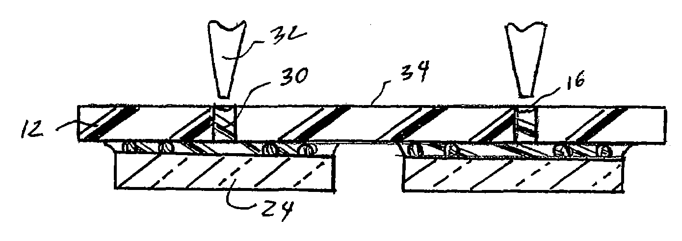
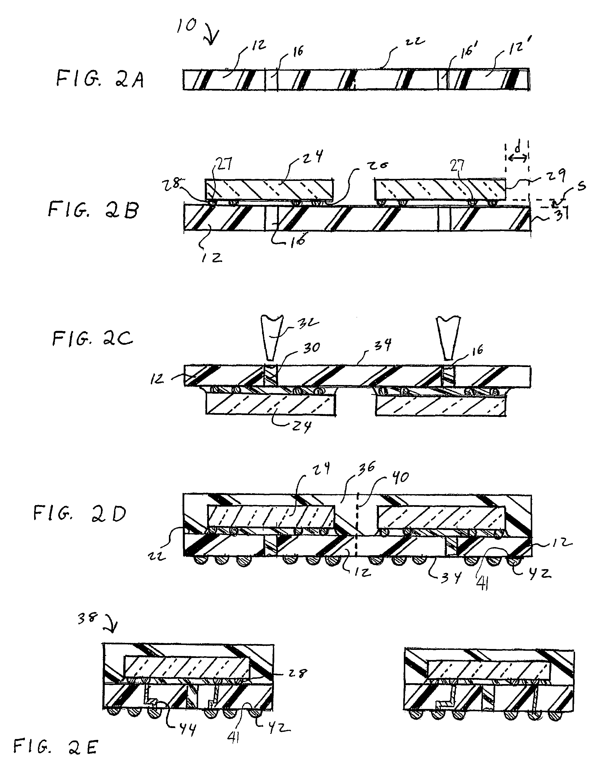
[0012]The details of one or more embodiments of the invention are set forth in the accompanying drawings and the description below. Other features, objects and advantages of the invention will be apparent from the description and drawings, and from the claims.
[0013]In accordance with a first embodiment of the invention, there is provided a method for the manufacture of a package to encapsulate at least one integrated circuit device. This method includes the steps of: (1) providing a dielectric substrate having a first plurality of bond pads formed on a first side thereof and at least one aperture; (2) electrically interconnecting the integrated circuit device to the plurality of bond pads forming a substrate/integrated circuit device assembly; (3) gravitationally aligning the substrate/integrated circuit assembly such that the integrated circuit device is lower than said substrate; (4) introducing a volume of a low viscosity dielectric into the at least one aperture, wherein the volume is effective to coat a surface of the integrated circuit device and substantially fill the at least one aperture; and

Problems solved by technology

The molding resin, typically a thermosetting epoxy, is applied at a relatively high temperature and velocity and could damage the semiconductor die or solder interconnects on impact.
This method has poor control of the spread of the underfill material and it is necessary for there to be up to three millimeters of clearance between the perimeter of the semiconductor die and the edge of the substrate to accommodate the underfill flow.
As a result, the length and width of the semiconductor package cannot be smaller than six millimeters plus the length and width of the semiconductor die.
Since air pockets are typically trapped between the integrated circuit and the substrate, the method is also prone to incomplete fill and voids that impact reliability.
Voids or incomplete fill could also occur due to the limited space between the semiconductor die and the substrate.
While it is known to use vacuum assisted molding, this is an expensive process and requires the use of molded compounds having a fine filler, on the order of less than 50 microns, to fill in the gap between the semiconductor die and substrate.

Method used


Image

  • Method of making flip-chip package with underfill
  • Method of making flip-chip package with underfill
  • Method of making flip-chip package with underfill

Examples


Embodiment Construction

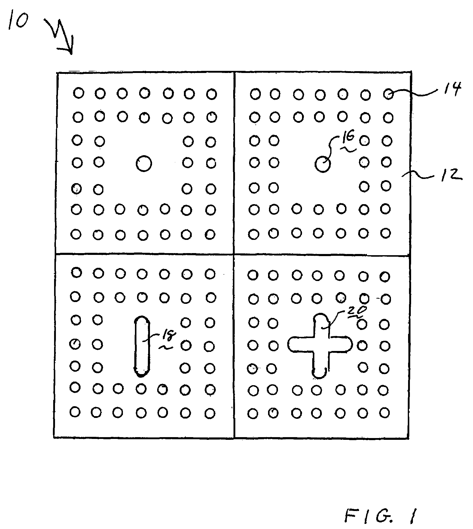
[0018]FIG. 1 shows a panel 10 containing a plurality of substrates 12 for use in the manufacture of a flip chip integrated circuit package in accordance with an embodiment of the invention. The substrate is formed from any suitable dielectric material such as FR-4, a flame resistant epoxy material. A first side of the substrate contains a first plurality of bond pads 14. The bond pads are metallized to be electrically conductive and wettable by the solder employed for the flip-chip bond. Typically, this solder is a lead-based or lead-free eutectic. The first plurality of bond pads 14 are arranged in an array to match an array of input / output pads on an electrically active face of an integrated circuit die. At least one aperture 16 extends through the substrate 12. As described hereinbelow, the aperture 16 functions as a gate to introduce a low viscosity underfill between the substrate 12 and the integrated circuit device. The number of apertures, the shape of the apertures and the c...


PUM


Abstract

A method for the manufacture of a package to encapsulate at least one integrated circuit device includes the steps of: (1) providing a dielectric substrate having a first plurality of bond pads formed on a first side thereof and at least one aperture; (2) electrically interconnecting the integrated circuit device to the plurality of bond pads forming a substrate / integrated circuit device assembly; (3) gravitationally aligning the substrate / integrated circuit assembly such that the integrated circuit device is lower than said substrate; (4) introducing a volume of a low viscosity dielectric into the at least one aperture, wherein the volume is effective to coat a surface of the integrated circuit device and substantially fill the at least one aperture; and (5) encapsulating the integrated circuit device and the first side of said substrate with a dielectric polymer.

Description

CROSS REFERENCE TO RELATED APPLICATION(S)[0001]This application claims the benefit of Non-Provisional application Ser. No. 11 / 705,318, filed on Feb. 12, 2007 entitled “Method of Making Flip-Chip Package with Underfill” and Provisional Application No. 60 / 773,269 filed on Feb. 14, 2006, entitled “Method of Making Flip-Chip Package with Underfill”, both of which are incorporated by reference in their entirety herein.U.S. GOVERNMENT RIGHTS[0002]Not ApplicableBACKGROUND OF THE INVENTION[0003]1. Field of the Invention[0004]This invention relates to a method for the manufacture of a package to encapsulate an integrated circuit device. More particularly, a chip-scale package is manufactured by flip-chip bonding input / output pads on the integrated circuit device to bond pads on a substrate. The substrate further includes at least one aperture to enable the introduction of a low viscosity dielectric between the substrate and the integrated circuit device. The bonded assembly is then encapsula...

Claims


Application Information

Patent Timeline
IPC IPC(8): H01L21/00H01L21/44H01L21/46
CPCH01L23/3128H01L21/565H01L2924/01322H01L2924/15311H01L2924/01087H01L2224/73204
Inventor SAN ANTONIO, ROMARICO SANTOSSUBAGIO, ANANGMACARAEG, GLENNBAJACAN RAMOS, MARY JEAN
Owner UNISEM M BERHAD
Learn More