Method of adaptively selecting chips for reducing in-line testing in a semiconductor manufacturing line
a semiconductor manufacturing line and chip technology, applied in semiconductor/solid-state device testing/measurement, testing circuits, instruments, etc., can solve the problems of inability to be disposed of due to cost, chips that are known to be bad may continue to be subjected to subsequent in-line tests, and inevitably misprocessed or affected by defects
- Summary
- Abstract
- Description
- Claims
- Application Information
AI Technical Summary
Benefits of technology
Problems solved by technology
Method used
Image


Examples
Embodiment Construction
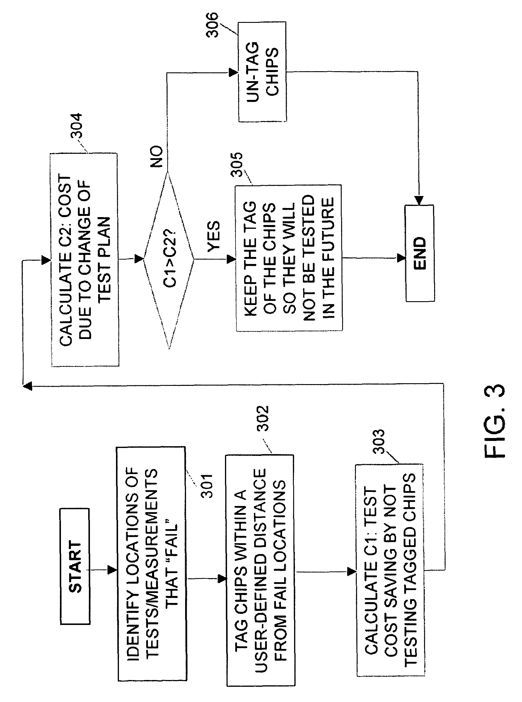
[0008]Accordingly, it is an object of the present invention to provide a system and a method for identifying defective chips early in a manufacturing process, bypassing testing potentially bad chips identified by their respective history of failing certain tests, and allowing only good chips to be further tested.
[0009]It is another object to limit further testing and measurements by taking into consideration the test history of, e.g., in-line tests and measurements during defect inspection (PLY), metrology, parametric, functional tests, wherein the health of a wafer is monitored as it move down a fabrication line.
[0010]It is still another object to reduce the testing time allocated to a wafer by disposing of the wafers or chips that inevitably are misprocessed or affected by defects as they move down a fabrication line.
[0011]It is a further object to provide a system and method that targets potentially bad chips that are excluded from further testing, and that selectively alters the...
PUM
 Abstract
Description
Claims
Application Information
 - R&D
- Intellectual Property
- Life Sciences
- Materials
- Tech Scout
- Unparalleled Data Quality
- Higher Quality Content
- 60% Fewer Hallucinations
Browse by: Latest US Patents, China's latest patents, Technical Efficacy Thesaurus, Application Domain, Technology Topic, Popular Technical Reports.
© 2025 PatSnap. All rights reserved.Legal|Privacy policy|Modern Slavery Act Transparency Statement|Sitemap|About US| Contact US: help@patsnap.com