
Input of test conditions and output generation for built-in self test

a built-in self test and output generation technology, applied in the field of memory devices, can solve the problems of increasing manufacturing problems, difficult to achieve perfect yields, and constant testing challenges for manufacturers, so as to improve bistability, reduce testing time, and reduce costs.

Active Publication Date: 2010-03-02
INFINEON TECH LLC
View PDF5 Cites 7 Cited by
  • Summary
  • Abstract
  • Description
  • Claims
  • Application Information

AI Technical Summary

Benefits of technology

[0021]The present invention provides an effective software controlled system and method that permits interactive adjustment of the various test conditions utilized by BIST test circuitry. It is an objective of the system and method of the present invention to provide the capability to adjust the test conditions via software control, thereby eliminating the need to do so via mask changes that may be prohibitively expensive and time consuming. It is another objective of the present invention to enable the interactive adjustment of test condition based on results executed as part of the BIST sort flow. It is still another objective of the invention to enable interactive adjustment of the internal voltage and current references to levels required for correct part operation and optimal part yield. Such interactive software control and adjustment of test conditions simplifies the use of BIST without the traditional mask changes. The test conditions determined during part characterization, debug, and the qualification process effectively provide for screening out parts which would eventually fail in later testing, or otherwise become reliability failures. A predefined sequence of global variables associated with the test conditions is communicated to a BIST interface circuit. The global variables comprise one or more bits of a multi-bit code representing a variable value associated with one or more BIST tests. The BIST interface is adapted to receive the variables and adjust corresponding test conditions based on the variable value. For example, a variable code “10” in the predefined sequence may represent a gate voltage of 3.7V used in one or more BIST tests.
[0023]In a preferred implementation of the present invention, the predefined global variable sequence is serially communicated to the BIST interface to minimize the number of test pins used in contact with the chip under test. Alternately, parallel communications and other forms of communication are contemplated in the context of the present invention. In yet another aspect of the invention, automatic test equipment may be used to communicate with the BIST interface. The BIST interface, then, establishes the conditions for one or more tests executed by the BIST circuit on one or more associated Flash memory circuits.
[0025]Typically, BIST uses a fixed set of test conditions, wherein the pass / fail test results will stand regardless of the application or conditions. By contrast, the present invention permits adjustment of the variables of the various test conditions to improve on the capabilities and flexibility of BIST. In this way, test conditions for the BIST tests can be adjusted as needed for the application.
[0031]In accordance with another aspect of the present invention, a method enables programmable self-test conditions by providing a BIST interface adapted to adjust a test condition used in a BIST circuit, providing a Flash memory comprising the sector of memory cells, providing the BIST circuit adapted to test the flash memory, communicating with the BIST interface one or more global variables associated with the test condition, adjusting the test condition used by the BIST circuit based on the values represented by the global variables, performing one or more test operations on the flash memory in accordance with the adjusted test condition, and reporting the results of the memory test operations. Thus, the method of the present invention tests a sector or array of memory cells utilizing BIST test circuitry having adjustable test conditions by communicating (e.g., serially) programmable (e.g., via ATE or other such test equipment) global variables to a BIST interface adapted to receive and adjust a variety of test conditions associated with the BIST tests. The present invention is implemented in a BIST circuit associated with the memory to reduce testing time, costs, and to improve on the capabilities and flexibility of BIST.

Problems solved by technology

However, due to the complex nature of today's integrated circuits and an attendant sensitivity to variations in manufacturing processes, manufacturers are constantly confronted with new testing challenges.
This testing is necessary because perfect yields are difficult to achieve.
It is not uncommon for a certain percentage of unpackaged ASIC die to contain memory cells which fail testing processes, due largely to non-systemic manufacturing defects.
Such manufacturing issues are likely to increase as process geometries continue to shrink and the density of memory cells increases.
The main disadvantage of using such standard test modes is that the test system must test the devices interactively.
Consequently, only a limited number of devices can be tested at a given time, and a significant amount of overhead time is incurred due to tester limitations (e.g., power up time is needed on certain pins while the mode is being accessed and while the tester is controlling the chip and checking the results).
Carefully trimming or controlling such bias and reference voltages is essential to proper memory operations, but requires considerable test time if conventional testers are used to test devices which do not have BIST.
With such an erase procedure, however, cells that are sufficiently erased initially will also be repeatedly erased, leading to some cells becoming “over-erased” before other cells are sufficiently erased.
An over-erased condition is undesirable for many reasons.
Regardless of the grouping selected, however, a truly representative erase threshold level for the sector or array of memory cells is elusive, as differences exist between memory arrays and / or the particular ASIC application wherein the array resides.
Further, the aforementioned grouping choices may not be sufficiently representative of the desired erase threshold level, and also may be difficult to implement in BIST circuitry.
As a result of the aforementioned tests required by BIST, implementing such test choices, voltages, and other variations in BIST circuitry traditionally requires mask changes that may be prohibitively expensive and time consuming.

Method used


Image

  • Input of test conditions and output generation for built-in self test
  • Input of test conditions and output generation for built-in self test
  • Input of test conditions and output generation for built-in self test

Examples


Embodiment Construction

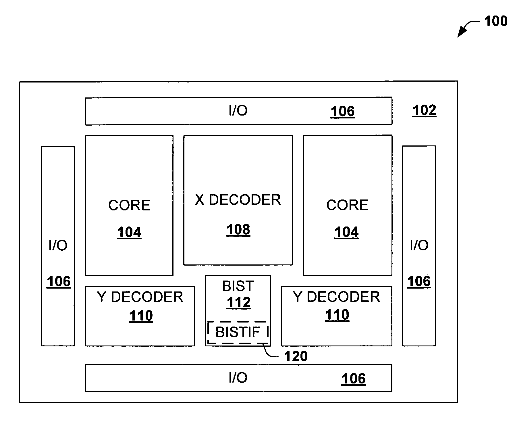
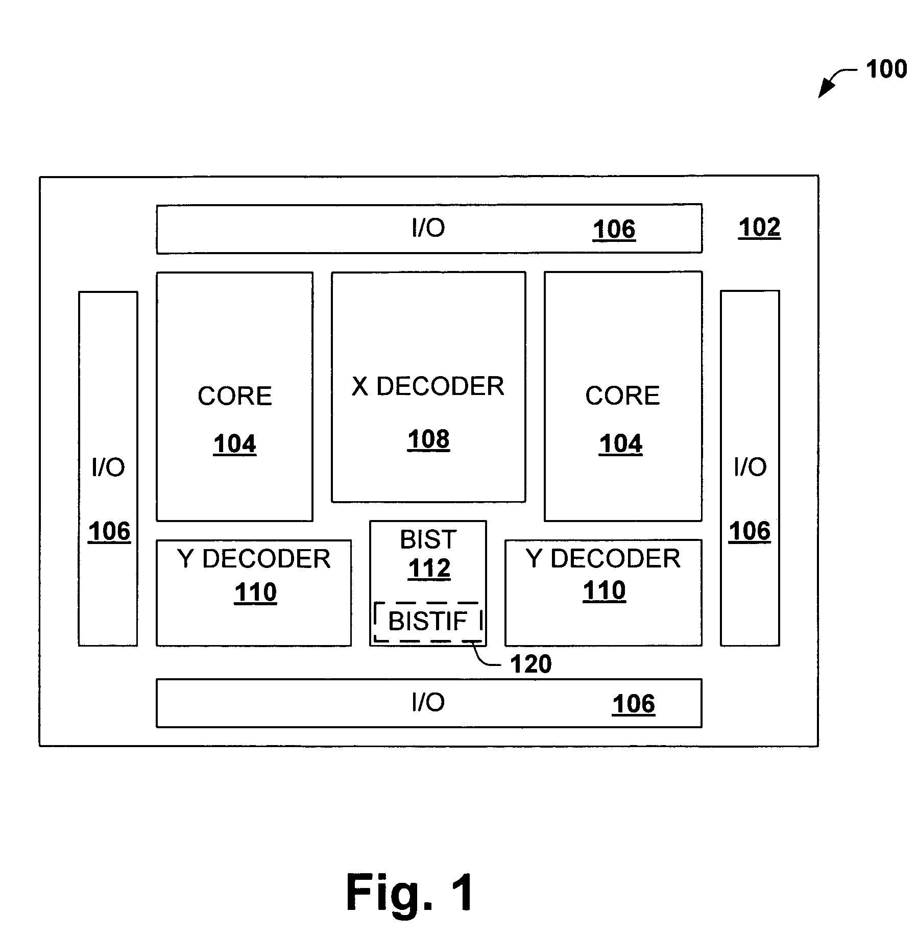
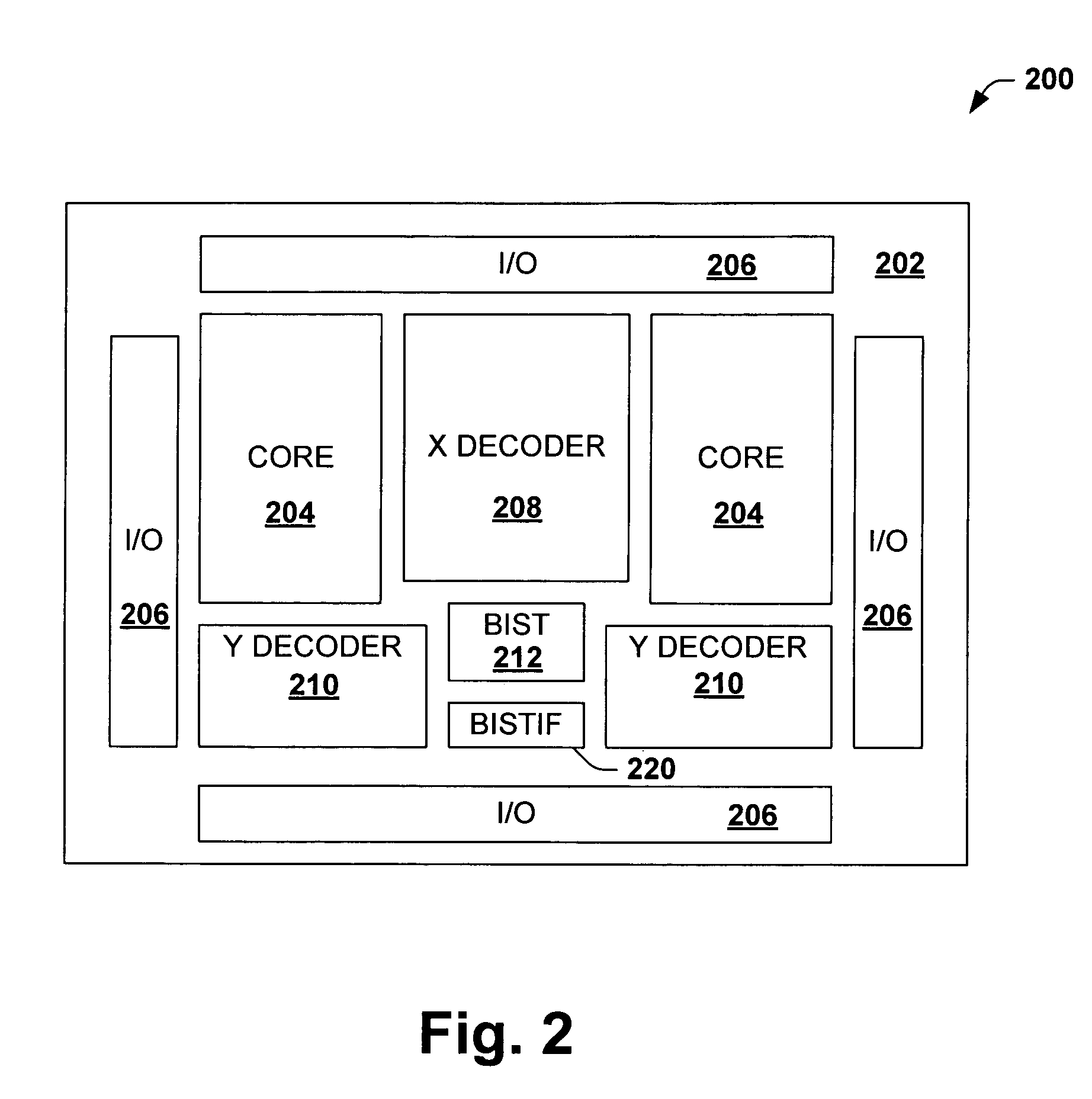
[0045]One or more aspects of the present invention are described with reference to the drawings, wherein like reference numerals are generally utilized to refer to like elements throughout, and wherein the various structures are not necessarily drawn to scale. In the following description, for purposes of explanation, numerous specific details are set forth in order to provide a thorough understanding of one or more aspects of the present invention. It may be evident, however, to one skilled in the art that one or more aspects of the present invention may be practiced with a lesser degree of these specific details. In other instances, well-known structures and devices are shown in block diagram form in order to facilitate describing one or more aspects of the present invention.

[0046]A self-test system and protocol may be used to program variable test conditions for a built-in self test circuit of a Flash memory device including a sector or an array of memory cells. The self-test pro...


PUM


Abstract

A system and method is discussed for providing programmable test conditions for a built-in self test circuit of a flash memory device. The present invention employs a flash memory having BIST circuit for testing the memory and a BIST interface circuit adapted to adjust the test conditions of the memory tests. The BIST interface circuit is operable to receive one or more global variables associated with the test conditions of a plurality of tests used on the flash memory and to output results of the memory tests based on the value of the variables. The global variables are used to adjust the test conditions and to trim one or more references used in various flash memory tests and operations. The system may further include a serial communications medium for communicating the global variables to the BIST interface and test results from the interface.

Description

RELATED APPLICATIONS[0001]This application is related to U.S. patent application Ser. No. 11 / 041,608 filed Jan. 24, 2005, which is entitled “AUTOMATED TESTS FOR BUILT-IN SELF TEST”.FIELD OF INVENTION[0002]The present invention relates generally to memory devices and the like, and in particular to a system and method of inputting programmable global variables to and obtaining output from built-in self test circuits for self testing flash memory products.BACKGROUND OF THE INVENTION[0003]Improvements in semiconductor processes are making possible integrated circuits of increasing size and complexity. The semiconductor processing technologies that produce these integrated circuits have advanced to the point where complete systems, including memories, can now be reduced to a single integrated circuit or application specific integrated circuit (ASIC) device. These integrated circuits (also referred to as “die” or “chips”) may use many functions that previously could not be implemented on ...

Claims


Application Information

Patent Timeline
Patent Type & Authority Patents(United States)
IPC IPC(8): G01R27/28
CPCG01R31/318511G11C29/12005G11C29/16G11C29/44G11C16/04
Inventor LEE, MIMIHAMILTON, DARLENECHEAH, KEN CHEONG
Owner INFINEON TECH LLC
Learn More