Semiconductor with reduced pad pitch
a semiconductor and pad technology, applied in the field of semiconductor devices with reduced pad pitch, to achieve the effect of reducing the possibility of causing, reducing the pitch of bonding pads, and reducing the size of semiconductor devices
- Summary
- Abstract
- Description
- Claims
- Application Information
AI Technical Summary
Benefits of technology
Problems solved by technology
Method used
Image

Examples
first embodiment
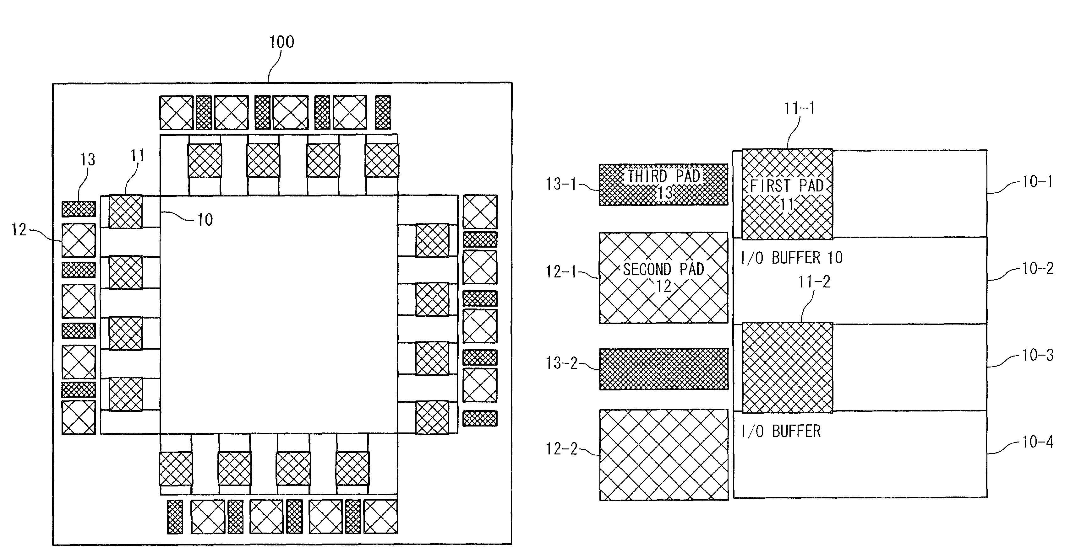
[0036]Referring not to FIG. 1, a semiconductor device according to the present invention includes an I / O buffer 10, a first pad 11, a second pad 12, and a third pad 13.
[0037]The semiconductor device 100 of this embodiment is provided with a rectangular semiconductor chip in which internal interconnection layers having a laminated structure of a plurality of layers and internal elements are formed, and includes various kinds of processing circuit inside, and includes the I / O buffer 10 on respective sides of circumference part. In addition, the first pad 11 is formed on an uppermost part in an area where the I / O buffer is formed. The second pad 12 and the third pad 13 are further formed outside the above-described area.
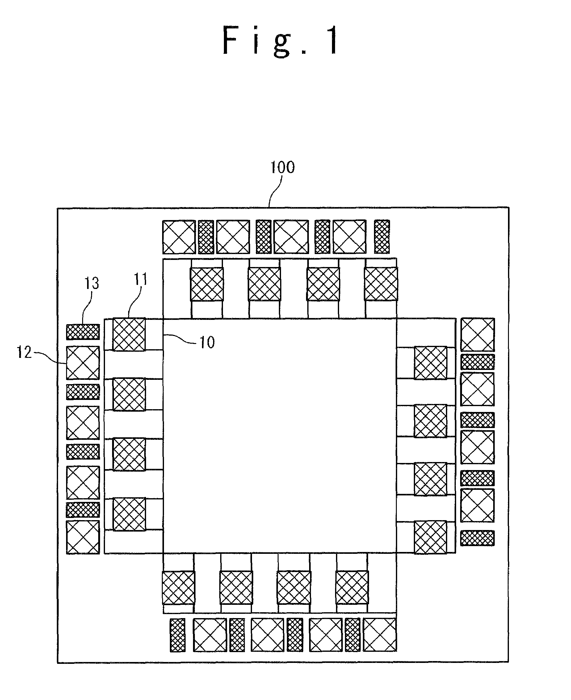
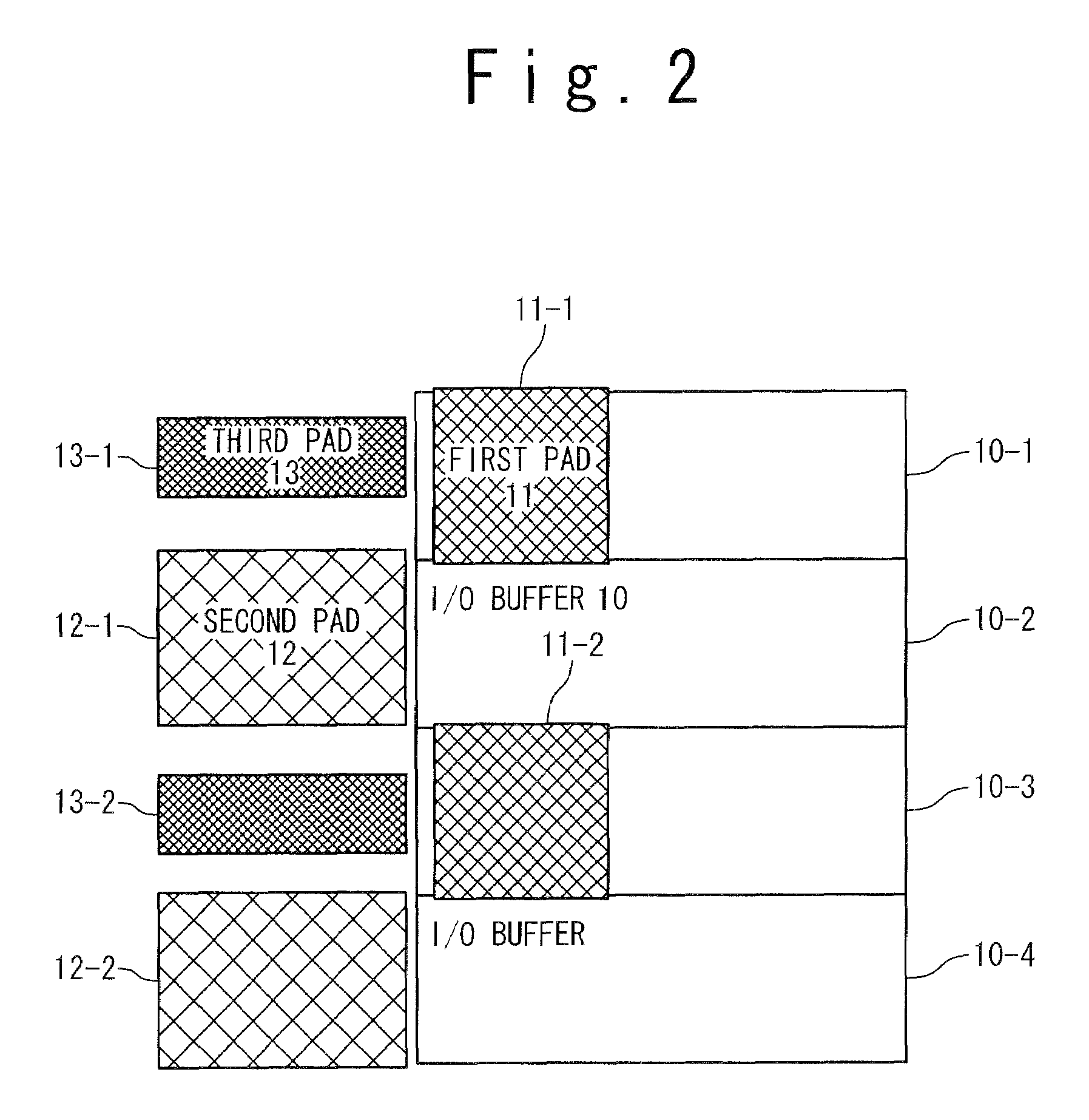
[0038]In FIG. 2, only a part of one side of the semiconductor device is shown to describe the first, second, and third pads for simplification.
[0039]Each I / O buffer 10-i (i=1 to n: n is an arbitrary natural number) of the I / O buffers 10 represents an inputting and outpu...
second embodiment
[0066]Referring to FIGS. 5A, 5B, and 5C, the present invention will be explained below.
[0067]The present embodiment contributes to a reduction of a chip size by arranging first pads 11, second pads 12 and third pads 13 on an I / O buffer 10 so that an area where only pads are formed on is reduced. A structure formed under the second pads and the third pads is durable against the impact of probing applied to the pads. That is to say, the structure includes a stress relaxation layer (stress absorbing layer). As an example of the stress absorbing layer, a layer on which no element or circuit is formed is provided just under the pad layer. Or the stress absorbing layer is an interconnection layer which is not used as a part of an electrical circuit of the semiconductor chip. Or structural material provided to form a metal layer does not exist in the stress absorbing layer. As another example of the stress absorbing layer, the stress absorbing layer can be constructed by a thick interlayer...
third embodiment
[0078]Referring to FIGS. 6, 7, and 8, the present invention will be explained below. When, of the I / O buffer 10 connected to the first pad 11, a buffer with a broader width than a pad pitch (a broad width macro) is arranged, for example, such as a macro with broad width (macro cell), the buffer can be arranged without changing a shape of the pad.
[0079]FIG. 6 shows a case where the first pad 11-1 is arranged on the I / O buffer 10-2 in a semiconductor device employing the broad width macro.
[0080]For example, as shown in FIG. 6, even when an I / O buffer 10-2 of the I / O buffers 10-1 to 10-5 is a broad width buffer, this broad width macro can be used as in the case of the normal I / O buffer 10-i (the width thereof is not broad). That is to say, in the present embodiment, a size of the I / O buffer can be changed within some degree of freedom, and an arrangement of respective pads do not depend on a relationship between position of each I / O buffer and position of each pad.
[0081]In addition, wh...
PUM
 Abstract
Description
Claims
Application Information
 - R&D
- Intellectual Property
- Life Sciences
- Materials
- Tech Scout
- Unparalleled Data Quality
- Higher Quality Content
- 60% Fewer Hallucinations
Browse by: Latest US Patents, China's latest patents, Technical Efficacy Thesaurus, Application Domain, Technology Topic, Popular Technical Reports.
© 2025 PatSnap. All rights reserved.Legal|Privacy policy|Modern Slavery Act Transparency Statement|Sitemap|About US| Contact US: help@patsnap.com