
Coating and developing apparatus, coating and developing method, and storage medium

a technology of developing apparatus and coating, applied in the direction of printers, instruments, photosensitive materials, etc., can solve the problems of increasing the load of the conveying arm and being more likely to cause a conveying error, and achieve the effect of suppressing the decrease of the wafer conveying accuracy

Active Publication Date: 2010-01-12
TOKYO ELECTRON LTD
View PDF4 Cites 24 Cited by
  • Summary
  • Abstract
  • Description
  • Claims
  • Application Information

AI Technical Summary

Benefits of technology

The present invention provides a coating and developing apparatus and method for coating and developing substrates with a resist and exposing them to light. The apparatus includes a carrier block, processing block, and interface block for conveying the substrates to and from the processing block. The processing block has multiple resist-film forming blocks and developing blocks, and the conveyance means for the substrates ensures that the substrates are conveyed one at a time in a conveying direction. The apparatus and method allow for improved control of substrate conveying speed, reducing decreases in conveyance accuracy. A storage medium containing a computer program is also provided for activating the coating and developing apparatus.

Problems solved by technology

However, there is the problem that for example, if the conveying speed of the conveyance arm 106 is raised to allow intermodule conveyance within 2 or 3 seconds for improved throughput, an increase in load of the conveyance arm 106 could be more likely to cause a conveying error such as a fall of the wafer from the conveyance arm 106 during conveyance.

Method used


Image

  • Coating and developing apparatus, coating and developing method, and storage medium
  • Coating and developing apparatus, coating and developing method, and storage medium
  • Coating and developing apparatus, coating and developing method, and storage medium

Examples


first embodiment

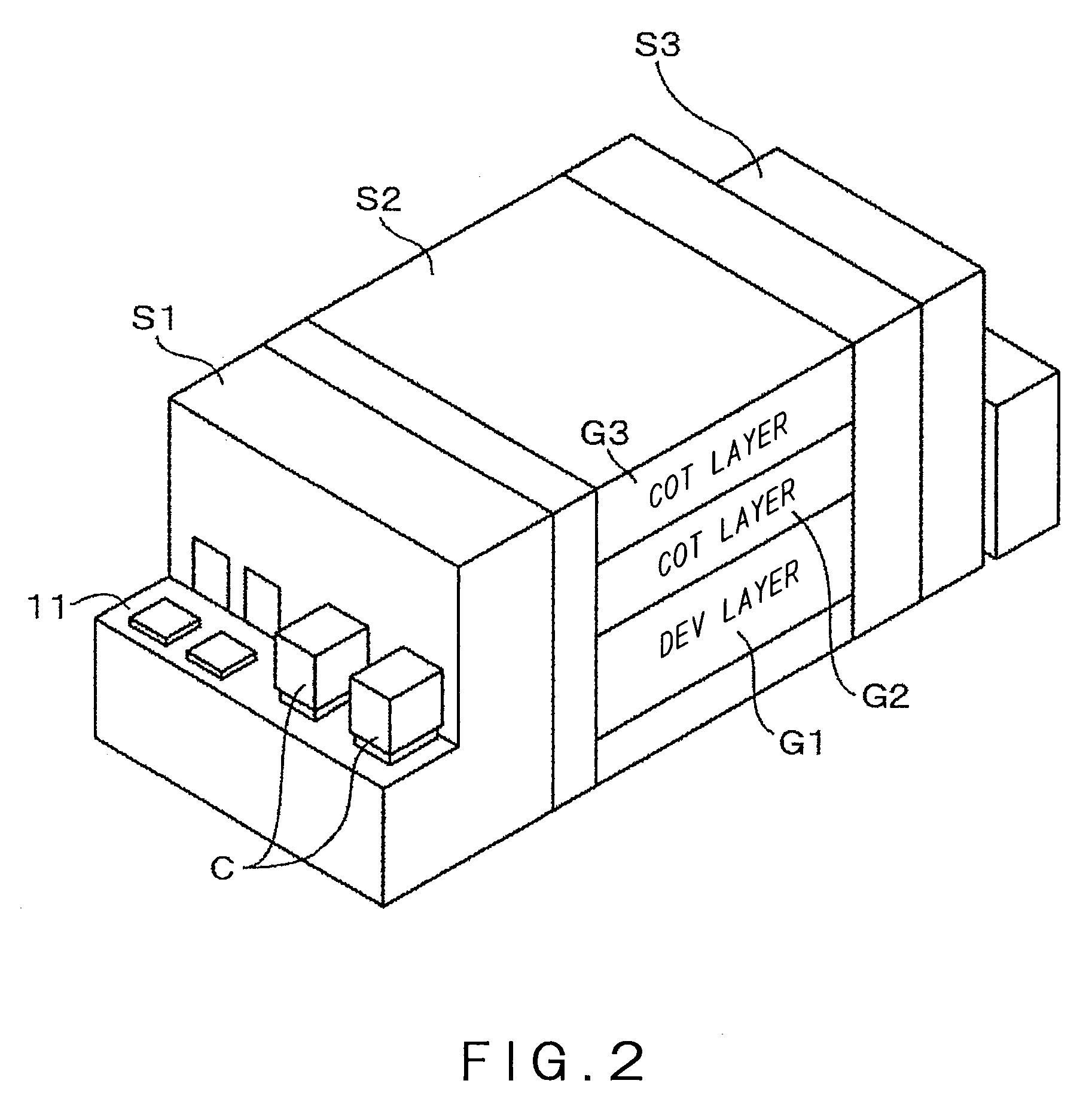
[0039]A coating and developing apparatus 1 that is a first embodiment is described below using FIGS. 1 to 3. FIG. 1 is a plan view of a system having an exposure apparatus S4 connected to the coating and developing apparatus 1. FIG. 2 is a perspective view of the system. FIG. 3 is a longitudinal plan view thereof.

[0040]The coating and developing apparatus 1 includes a carrier block S1, which includes carrier-mounting tables 11 and a transfer arm 12. The transfer arm 12 in the carrier block S1 is constructed to remove wafers W from hermetically sealed carriers C mounted on each table 11, and then transfer each wafer W to a processing block S2 adjacent to the carrier block S1. The transfer arm 12 that functions at this time as a conveyance element for loading the wafer W into the processing block S2 is hereinafter referred to as the processing block loading conveyance element. In addition, the transfer arm 12 is constructed to receive a processed wafer W from the processing block S2 a...

second embodiment

[0088]A second embodiment is described below referring to FIGS. 9 and 10. A coating and developing apparatus 6 according to the second embodiment of FIGS. 9 and 10 differs from the coating and developing apparatus 1 according to the above first embodiment in that a COT layer G4 constructed similarly to the COT layers G2, G3 is stacked on the COT layer G3.

[0089]As shown in FIGS. 9, 10, the COT layer G4 includes ADH modules 51A, 51B, COT modules 53A to 53C, heating modules 54A to 54D, a WEE module 55, and a conveyance arm E4, at positions equivalent to those of the ADH modules 21A, 21B, COT modules 23A to 23C, heating modules 24A to 24D, WEE module 25, and conveyance arm E2 of the COT layer G2.

[0090]In addition, in positions of the shelf unit U5 that are equivalent to those of the COT layer G4, cooling module CPL52A, a transfer stage TRS8, cooling module CPL52B, and a buffer module BM56 are provided in stacked form in that order from below. These modules are equivalent to those of the...

third embodiment

[0093]A coating and developing apparatus 7 that is a third embodiment is described below referring to FIGS. 11 and 12. The coating and developing apparatus 7 according to the third embodiment, shown in FIGS. 11 and 12, includes a DEV layer G5 between the COT layer G2 and the DEV layer G1.

[0094]The DEV layer G5 is substantially of the same configuration as that of the DEV layer G1, and includes HP modules 61A to 61F, HP modules 64A to 64F, and a conveyance arm E5 at respective positions equivalent to those of the above-described HP modules 41A to 41F, HP modules 44A to 44F, and conveyance arm E1.

[0095]In addition, in positions of the shelf unit U6 that are equivalent to those of the COT layer G5, CPL62A, CPL62B, TRS9, and TRS10 equivalent to the CPL42A, CPL42B, TRS4, and TRS5, respectively, of the DEV layer G1, are provided in stacked form in that order from below. Furthermore, the interface arm I can convey wafers W to the above modules. Besides, in this example, the shuttle arm 16 ...


PUM


Abstract

Disclosed herein is a coating and developing apparatus 1 whose decreases in substrate-conveying accuracy can be suppressed. A processing block S2 of the coating and developing apparatus 1 includes multiple resist-film forming blocks G2, G3, and a developing block G1. A conveyance element 12 for substrate loading into the processing block S2 is provided to convey substrates W from a carrier C to the resist-film forming blocks G2, G3. Also, a conveyance element I for substrate loading into an exposure apparatus S4 is provided in an interface block S3 to load the substrates W into the exposure apparatus S4 and after unloading the substrates W from the exposure apparatus S4, convey the substrates W to the developing block G1. The processing block loading conveyance element 12 conveys the substrates W, one at a time, from the carrier C to each resist-film forming block G2, G3, sequentially and periodically, and the exposure apparatus loading conveyance element I loads the substrates W from each resist-film forming block G2, G3 into the exposure apparatus S4 in the sequence that each has been conveyed to the resist-film forming block G2, G3 by the processing block loading conveyance element 12.

Description

CROSS-REFERENCE TO RELATED APPLICATIONS[0001]The present patent application benefits from the Japanese Patent Application, Ser. No. JP-2007-221609, filed on Aug. 28, 2007, the disclosure of which is hereby incorporated by reference in its entirety.BACKGROUND OF THE INVENTION[0002]1. Field of the Invention[0003]The present invention relates to a method and apparatus for coating a substrate surface such as a semiconductor wafer or liquid-crystal display (LCD) glass substrate surface, with a resist liquid and developing the substrate after exposure thereof to light. The invention also concerns a storage medium used for these coating and developing operations.[0004]2. Description of the Related Art[0005]In a photoresist process that is one of semiconductor-manufacturing processes, the surface of a semiconductor wafer (hereinafter, also referred to simply as a wafer) is coated with a resist, and then after exposure of this resist on the wafer to light with a required pattern, the wafer i...

Claims


Application Information

Patent Timeline
Patent Type & Authority Patents(United States)
IPC IPC(8): G03D5/00B05C13/00B65H11/00G03B27/32
CPCG03F7/70525G03F7/7075G03F7/70808H01L21/6715H01L21/67225H01L21/67745Y10S414/14B05C11/10
Inventor HARA, YOSHITAKAKATSUKI, SHINGO
Owner TOKYO ELECTRON LTD
Learn More