
Electronic device, package having the same, and electronic apparatus

a technology of electronic devices and circuit elements, applied in the direction of semiconductor devices, cooling/ventilation/heating modifications, semiconductor/solid-state device details, etc., can solve the problems of reducing the mobility of electrons (holes) in the channel, the thickness of the substrate is too thick to improve the heat radiation efficiency, and the performance of the cmos transistor degrades, so as to prevent prevent the degradation of the electric characteristic, and increase the operation frequency

Inactive Publication Date: 2010-01-05
FUJITSU LTD
View PDF23 Cites 2 Cited by
  • Summary
  • Abstract
  • Description
  • Claims
  • Application Information

AI Technical Summary

Benefits of technology

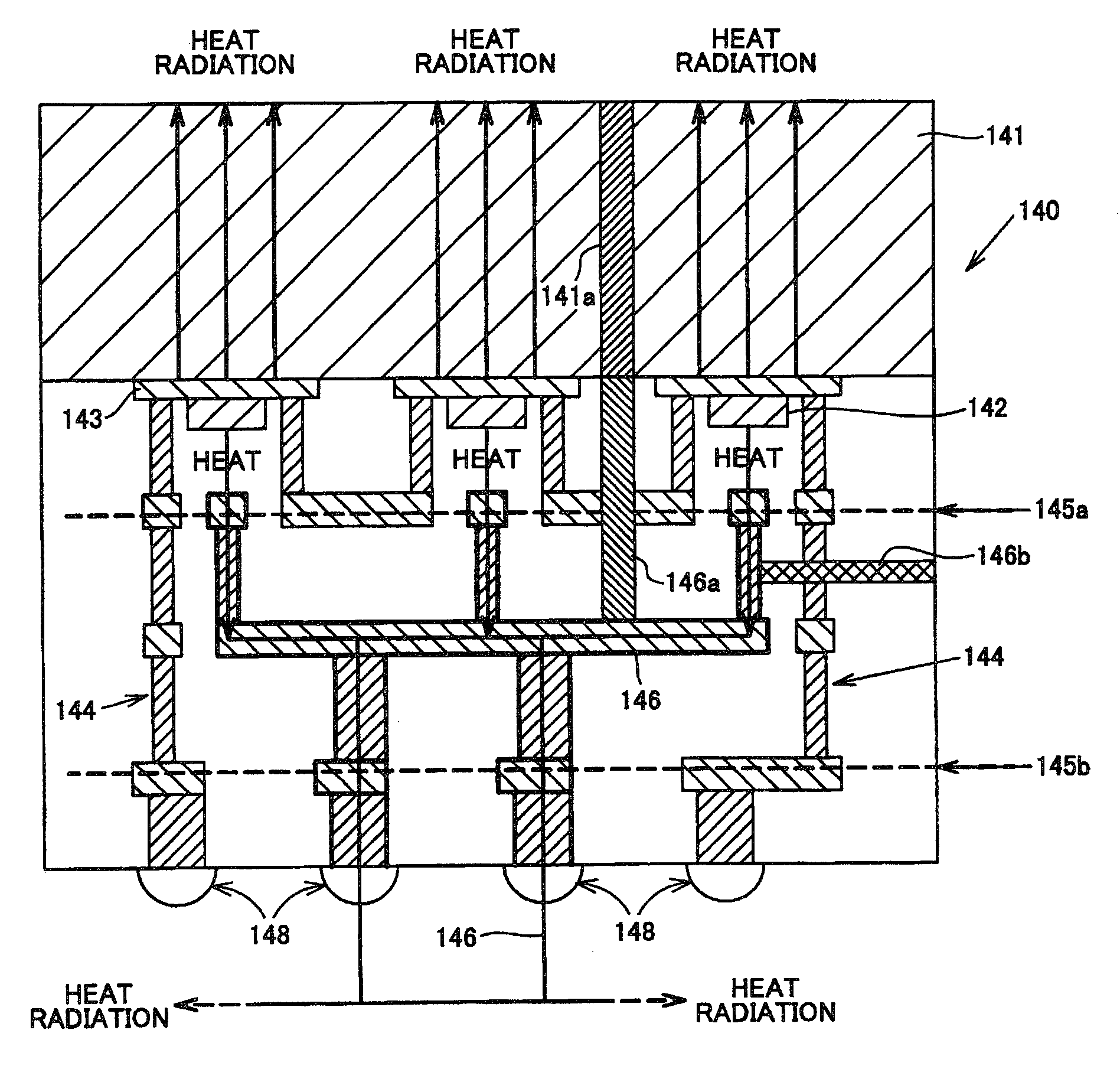
[0009]According to one aspect of the present invention an electronic device include a circuit element that transmits a signal to an external board and receives the signal from the external board, a signal wire that connects the external board to the circuit element, and a heat radiation wire that thermally contacts the circuit element, and radiates heat from the circuit element. This electronic device uses the heat radiation wire to protect the circuit element from thermal damages, and to maintain the electric characteristic. Therefore, this electronic device can use of a Low-k interlayer film material, and a higher operational frequency. The heat radiation wire may be electrically insulated from the circuit element. Thereby, the heat radiate wire can prevent degradations of the electric characteristic of the circuit element.
[0010]The heat radiation wire may be electrically isolated from the circuit element. The electronic device may further include a bump that is connectible to the external board, wherein the heat radiation wire is thermally connected to the bump. In this case, the bump serves as a thermal exhaust port. The electronic device may further include plural bumps that are connectible to the external board, wherein the signal wire and the heat radiation wire are connected to different bumps among the plural bumps. Use of different bumps prevents degradations of the electric characteristic of the circuit element. Use of the bump that is inherently provided on the chip does not increase the number of components, and maintains the size of the chip.
[0011]The heat radiation wire may be made of a metallic material having a high thermal conductivity, such as cupper and aluminum. When the heat radiation wire is made of the same material as that of the signal wire, the same machine can form both the signal wires and the heat radiation wires as dummy wires. The heat radiation wire may have the same diameter as that of the signal wire. It is conceivable to make a diameter of the heat radiation wire greater than that of the signal wire so as to enhance the heat radiation efficiency, but this configuration would increase the size of the chip. However, the present invention allows the diameter of the heat radiation wire to be greater than the signal wire, when the large size of the chip is permissible or when the enhanced heat radiation efficiency is highly required.
[0012]The heat radiation wire may have a part that is spaced from the circuit element and extends parallel to a surface of the circuit element. Spacing from the circuit element can prevent the heat radiation wire from deteriorating the electric characteristic of the circuit element. A parallel arrangement to the surface of the circuit element rather than a perpendicular arrangement to the surface of the circuit element enables the heat radiation wire to uniformly receive the heat from the circuit element in a direction in which the heat radiation wire extends.
[0013]The electronic device may further include a dispersion member that is connected to the heat radiation wire, and disperses heat from the heat radiation wire. The dispersion member is, for example, a meshed member. The dispersion member can make the heat radiation efficiency uniform in the electronic device plane. The mesh structure permits the signal wires to pass through it, and a plate may be used instead of the mesh in an area that has no signal wires. The dispersion member may be formed in a wiring layer farthest from the circuit element among wiring layers of the signal wire. Thereby, the heat radiation efficiency in the final layer can be made uniform in the electronic device plane.

Problems solved by technology

In general, as the temperature of a CMOS transistor rises, the mobility of electrons (holes) in a channel lowers and the performance of the CMOS transistor degrades.
On the other hand, the substrate is too thick to improve the heat radiation efficiency.
In particular, in the SOI technology, the heat radiation by the self-heating substrate is insufficient.
In addition, a Low-k interlayer film material, such as SiLK, which is used to reduce the wiring parasitic capacity, contains air bubbles in its inside, and exhibits poor heat conductions.
As a result, as shown in FIG. 8, the heat exhausts near the transistor become insufficient.

Method used


Image

  • Electronic device, package having the same, and electronic apparatus
  • Electronic device, package having the same, and electronic apparatus
  • Electronic device, package having the same, and electronic apparatus

Examples


Embodiment Construction

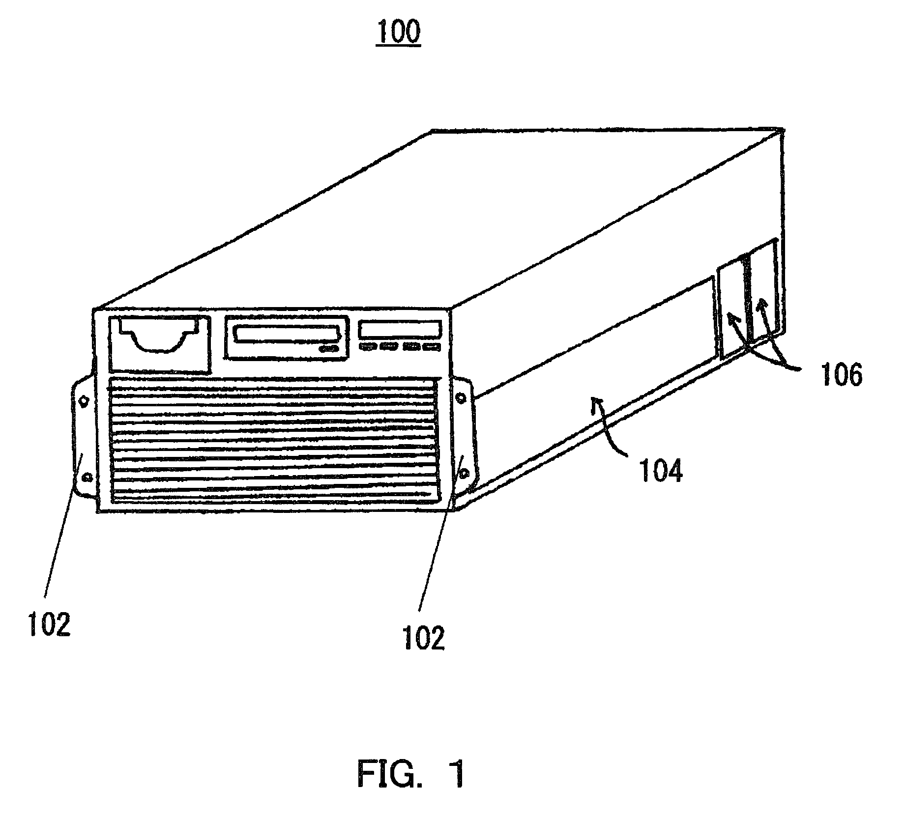
[0026]Referring now to the accompanying drawings, a description will be given of an electronic apparatus 100 according to one embodiment of the present invention. Here, FIG. 1 is a schematic perspective view of the electronic apparatus 100. As shown in FIG. 1, the electronic device 100 is implemented as a rack-mount type UNIX server. The electronic device 100 is screwed on a rack (not shown) by a pair of attachment parts 102, and mounted with a printed board 110 shown in FIGS. 2A-2C in a housing 104. The housing 104 has a fan module 106, in which a built-in cooling fan rotates to generate the airflow and compulsorily cools a built-in heat sink.

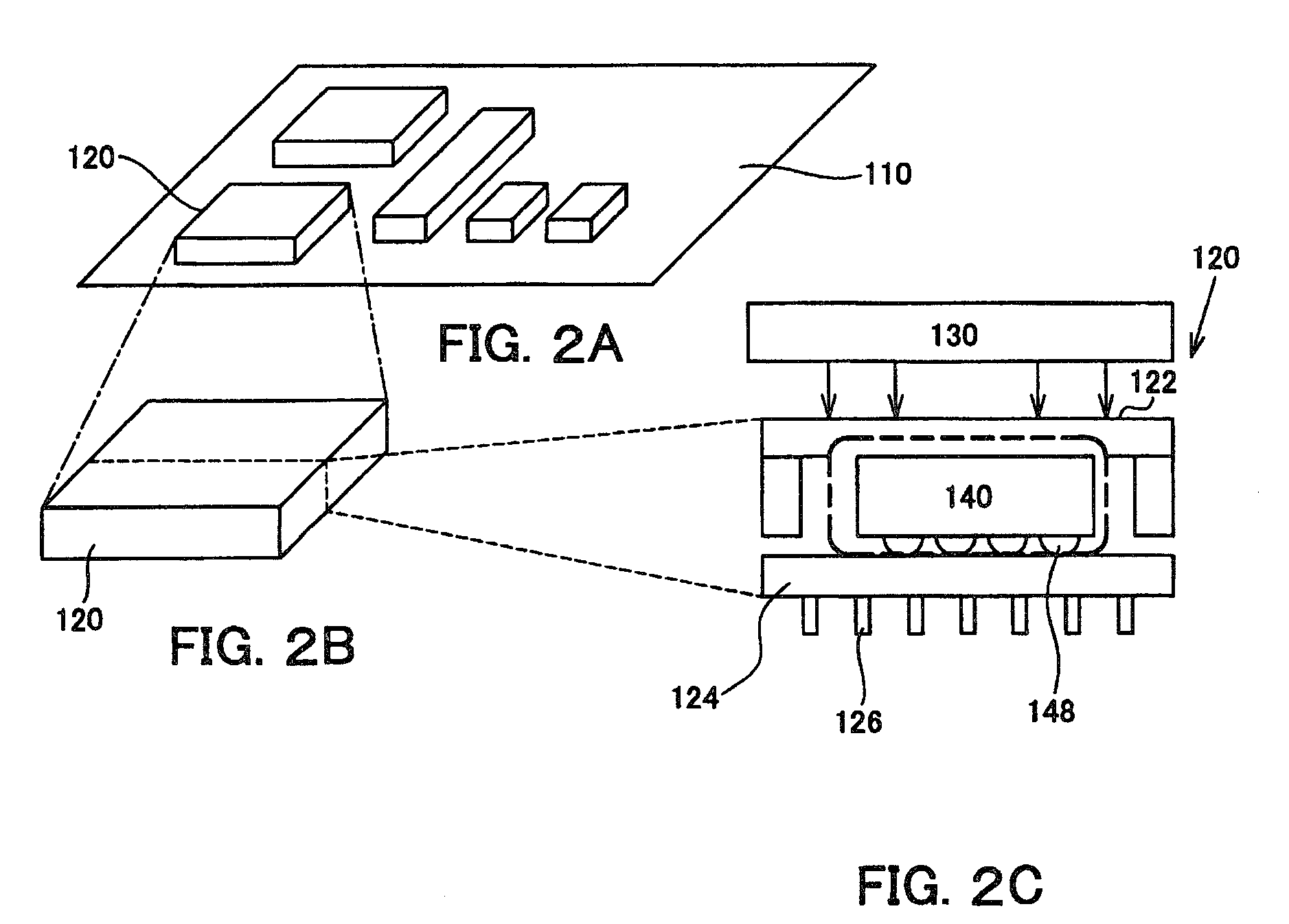
[0027]The printed board 110 includes a package (electronic component) 120, plural block plates (not shown), into which a memory card is to be inserted, and one or more connectors (not shown) for use with external units, such as a hard disc drive (“HDD”) and a LAN. The package 120 can use any one of a BGA, an LGA, and a PGA.

[0028]FIG. 2A is a s...


PUM


Abstract

There is provided an electronic device that includes a circuit element that transmits a signal to an external board and receives the signal from the external board, a signal wire that connects the external board to the circuit element, and a heat radiation wire that thermally contacts the circuit element, and radiates heat from the circuit element.

Description

CROSS-REFERENCE TO RELATED APPLICATIONS[0001]This application is a continuation claiming a foreign priority benefit based on PCT / JP2005 / 21053, filed on Nov. 16, 2005, which is hereby incorporated by reference herein in its entirety as if fully set forth herein.BACKGROUND OF THE INVENTION[0002]The present invention relates generally to an electronic apparatus that houses a circuit element, such as an LSI, and more particularly to a heat radiation structure for the circuit element that generates heat when it is operating. The present invention is suitable, for example, for heat radiations for LSI chips in a wide variety of packages, such as a ball grid array (“BGA”), a land grid array (“LGA”), and a pin grid array (“PGA”).[0003]Along with recently widespread, small and sophisticated electronic apparatuses, a supply of an electronic apparatus that realizes high density mounting is increasingly demanded. In order to meet this demand, a BGA package is conventionally proposed. In general,...

Claims


Application Information

Patent Timeline
Patent Type & Authority Patents(United States)
IPC IPC(8): H05K7/20
CPCH01L23/3677H01L23/49822H01L23/49816H01L2924/00014H01L24/48H01L2224/48227H01L2924/15311H01L2224/451H01L2224/45147H01L2224/45124H01L24/45H01L2924/12041H01L2924/181H01L2924/207H01L2924/00H01L2924/0002H01L2924/00015H01L2224/05599
Inventor TOKUNAGA, KENJI
Owner FUJITSU LTD
Learn More