
Semiconductor devices with inductors

a technology of inductors and semiconductor devices, which is applied in the direction of transformers/inductance details, transformer/inductance coils/windings/connections, basic electric elements, etc., can solve the problems of deterioration of input sensitivity, output of unwanted noise, and inability to use semiconductor devices

Active Publication Date: 2010-01-05
RENESAS ELECTRONICS CORP
View PDF18 Cites 16 Cited by
  • Summary
  • Abstract
  • Description
  • Claims
  • Application Information

AI Technical Summary

Benefits of technology

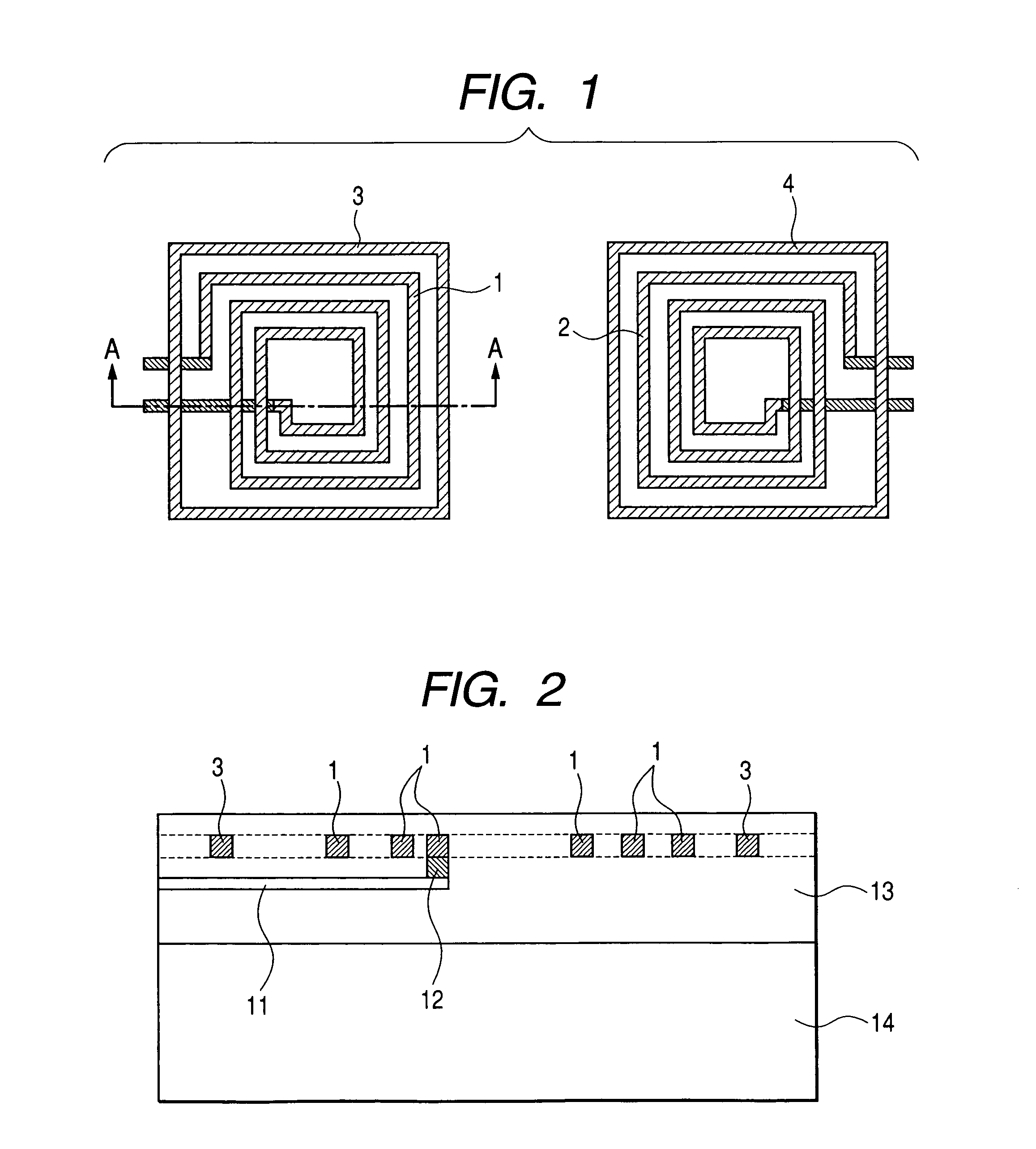
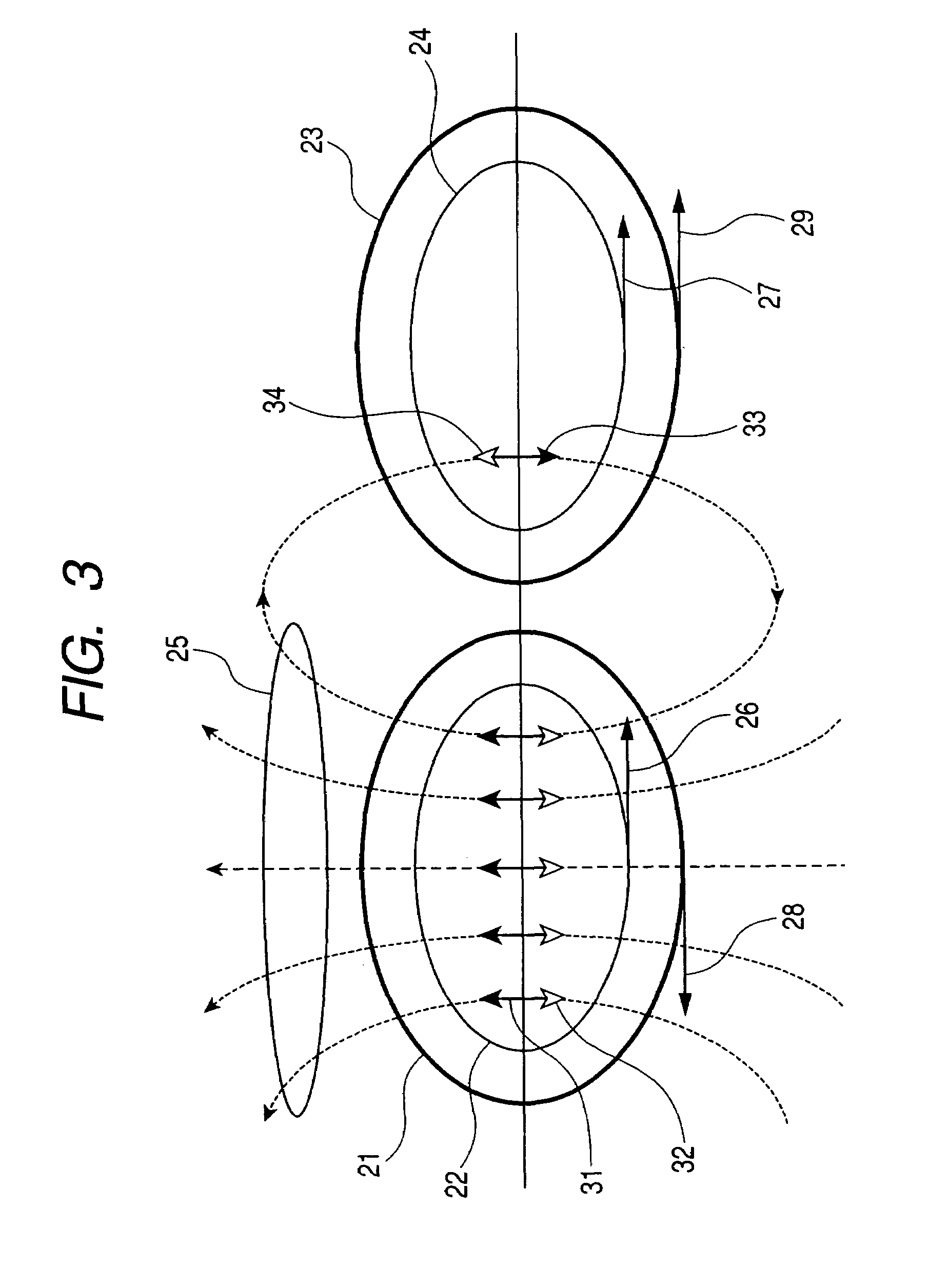
[0014]Accordingly, a technique is sought that reduces interference, caused by signal leakage among circuits, that is generated within the semiconductor device. As mentioned earlier, in the Patent Document 1, a method is disclosed for blocking interference signals transmitted through a semiconductor substrate, but it cannot restrain the effect brought about by the mutual inductance between inductors.
[0016]The effect brought about by magnetic fields generated in the vicinity of the inductors is reduced as the distance between an observation point and the respective inductors increases, as disclosed in the Non-Patent Document 2 in reference to the Biot-Savart law. Accordingly, countermeasures are conventionally, taken such as establishing a wire prevention region in the surrounding area of the respective inductors so as to separate inductors and wires from one another that are vulnerable to interference. However, such countermeasures have drawbacks, because such a wire prevention region requires extra room in the semiconductor device, which hampers efforts to increase the integration density and prevents a reduction in the layout size of the substrate.
[0018]The method as described in the Non-Patent Document 1, and as shown in FIG. 13, whereby the respective inductors, which are enclosed with grounded wires having a large width and are made of metal layers, is feasible to attenuate interference caused by mutual inductance. However, this method has the following drawbacks. The first problem is that the ground wires 7 and 9 used to be grounded in such an ideal manner that there is no potential fluctuation in those wires. For a semiconductor device, it is hard to make the impedance of the respective ground wires lower over wide range of frequency, because a parasitic element, such as a bonding wire, exists therein. Accordingly, signals with a voltage amplitude occur even on such ground wires. Further, such ground wires act as a common terminal between circuits, so that the signals generated in one circuit or another easily interfere with the inductors. The second problem is that disposing a wire which occupies a large area around the respective inductors, for the purpose of insuring that the respective ground wires come closer to an ideal grounding condition, causes a parasitic capacity on a semiconductor substrate. As a result, an induced current generated on the respective ground wires becomes hard to flow, thereby to minimize the effect on interference attenuation brought about by such induced current.
[0022]As will be mentioned later, the enclosure formed around the respective inductors by the closed loop wire attenuates the interference caused by mutual inductance. The first through third circuits are realized as a modulator circuit, a demodulator circuit and a local oscillator, respectively, which circuits are formed as high-frequency circuits, in which inductors are provided. Even when such high-frequency circuits are integrated into one semiconductor device, so that the respective circuits are disposed adjacently, the attenuation of interference caused among the circuits allows a high-performance in the operation of such high-frequency circuits that are incorporated into a semiconductor device.

Problems solved by technology

Although an inductor, which is one of the fundamental passive elements of a circuit, is used widely in an oscillator, a filter, a matching circuit, a transformer and so forth, it is scarcely used for a semiconductor device produced by a common method because of the difficulty in obtaining a larger inductance.
Thus, the result is that the inductors and the circuits are disposed nearby therein, so that problems occur, such as signal interference between inductors and interference between inductors and wires.
The occurrence of such signal interference within the semiconductor device invites a possibility of malfunction of the circuits, an output of unwanted noise and deterioration of the input sensitivity.
Thus, when there is interference between the local oscillator signals and the RF signals, serious intermodulation distortion and undesired leakage of disturbing waves will typically occur.
It is hard to improve the signals by use of a filter once they are subjected to intermodulation distortion owing to interference, since interference signal components exist within the same frequency band as the desired signals.
Furthermore, if interference occurs on a route through a parasitic element, it is impossible to incorporate an element in the circuit to hamper interference in the course of such route.
As mentioned earlier, in the Patent Document 1, a method is disclosed for blocking interference signals transmitted through a semiconductor substrate, but it cannot restrain the effect brought about by the mutual inductance between inductors.

Method used


Image

  • Semiconductor devices with inductors
  • Semiconductor devices with inductors
  • Semiconductor devices with inductors

Examples


first embodiment

[0056]FIG. 10 shows a first embodiment of the present invention. In this embodiment, inductors provided with wires for reducing the inductive coupling in the modulator circuit 97 are exemplified. In the drawing, reference numerals 61 and 62 respectively indicate inductors, reference numeral 63 indicates a wire for reducing the inductive coupling in the form of a closed loop wire, reference numeral 64 indicates a modulator, reference numerals 66a through 66d respectively indicate buffers, reference numerals 67a and 67b respectively indicate base band signal inputs, reference numerals 68a and 68b respectively indicate carrier wave inputs, reference numeral 69a and 69b indicate RF signal outputs and reference numeral 70 indicates a capacitor. Base band signals orthogonal to each other are input to the base band signal inputs 67a and 67b. The respective orthogonal base band signals are in the form of bipolar differential signals whose polarity is inverse relative to each other. Carrier ...

second embodiment

[0060]FIG. 11 shows the second embodiment of the present invention. In this embodiment, inductors provided with a wire for reducing the inductive coupling in the local oscillator 98 are exemplified. In the drawing, an inductor 71 acting as a choke coil, a wire 72 for reducing the inductive coupling in the form of a closed loop wire, a resonance inductor 73 of an oscillator, a varactor diode 74 of variable capacity, a capacitor 75, a transistor 76, a variable current source 77 to define the operational current of the transistor, a power source 78 to supply a voltage to the transistor 76, a frequency controller 79, an oscillator output 80 and a ground 81. In this embodiment, the inductor (i.e. choke coil) 71 takes the interfered with side.

[0061]The oscillation frequency is defined by the frequency of is a resonance circuit including the indicators 73, varactor diodes 74 and capacitors 75. When a control voltage is provided to the frequency controller 79, the bias voltage charged to th...

third embodiment

[0064]FIG. 12 shows a third embodiment of the present invention. In this embodiment, inductors provided with a wire for reducing the inductive coupling in the modulation circuit 97 and the local oscillator 98 are exemplified. The inductors of the modulator circuit 97 take the interference source side, while those of the local oscillator 98 take the interfered with side. In the drawing, numeral reference 91 indicates an RF variable gain amplifier, reference numerals 92a and 92b indicate base band filters, reference numerals 93a and 93b indicate base band amplifiers, reference numeral 94 indicates a frequency divider, reference numeral 95 indicates an RF output, reference numerals 96a and 96b indicate base band signals, reference numeral 97 indicates a modulator circuit and reference numeral 98 indicates a local oscillator.

[0065]The modulator circuit 97 has the same arrangement as that 25 of the first embodiment, and the variable frequency oscillator 98 has the same arrangement as tha...


PUM

PropertyMeasurementUnit
frequencyaaaaaaaaaa
frequencyaaaaaaaaaa
frequencyaaaaaaaaaa

Abstract

Semiconductor devices are provided with high performance high-frequency circuits in which interference caused by inductors is reduced. In a semiconductor device including a modulator circuit to modulate a carrier wave by a base band signal to output an RF signal and a demodulator circuit to demodulate the RF signal by use of the carrier wave to gain the base band signal and a local oscillator to generate the carrier wave, inductors respectively having a closed loop wire are adopted. Interference caused by mutual inductance is reduced by the closed loop wire. For example, where inductors are adopted in the modulator circuit, a closed loop wire is disposed around the outer periphery of the inductors.

Description

CLAIM OF PRIORITY[0001]The present application claims priority from Japanese application JP 2004-240569, filed on Aug. 20, 2004, the content of which is hereby incorporated by reference into this application.FIELD OF THE INVENTION[0002]The present invention relates in general to semiconductor devices with inductors, and, more specifically, the invention relates to semiconductor devices that are suitable for use in the high frequency circuits of a wireless communication device.BACKGROUND OF THE INVENTION[0003]An inductor for use in a circuit, in which high frequency 20 signals in the vicinity of the GHz band are received and transmitted, can be incorporated into a semiconductor device because of its smaller inductance. In this case, there are some countermeasures that can be used against the problem brought about by the fact that other inductors and wires, etc., may be disposed close to the inductor located within a minute interior of the semiconductor device. For example, an integra...

Claims


Application Information

Patent Timeline
Patent Type & Authority Patents(United States)
IPC IPC(8): H01L27/00H01F27/28
CPCH01L23/5227H03B5/1228H03B5/1215H03B5/1243H03B5/1271H01F17/0006H01L2924/3011H01L2924/0002H01L2924/00
Inventor SHIRAMIZU, NOBUHIRONAKAMURA, TAKAHIROMASUDA, TORUKASA, NOBUHIROMORI
Owner RENESAS ELECTRONICS CORP
Learn More