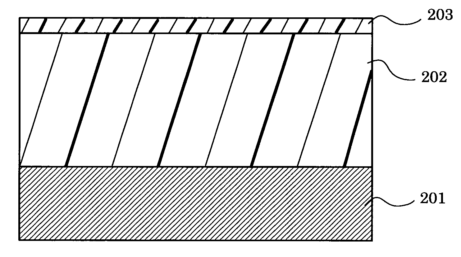
Photoconductor, manufacturing method thereof, image forming process and image forming apparatus using photoconductor, and process cartridge
a manufacturing method and photoconductor technology, applied in the direction of electrographic process apparatus, instruments, corona discharge, etc., can solve the problems of higher wear rate of photoconductors, less durability of organic photoconductors, and high surface layer wear, so as to achieve high and stable scratch resistance, high and stable wear resistance, and advantageous electrical properties
- Summary
- Abstract
- Description
- Claims
- Application Information
AI Technical Summary
Benefits of technology
Problems solved by technology
Method used
Image
Examples
example 1
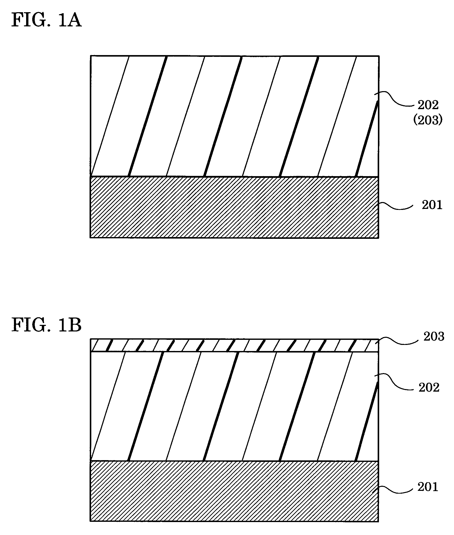
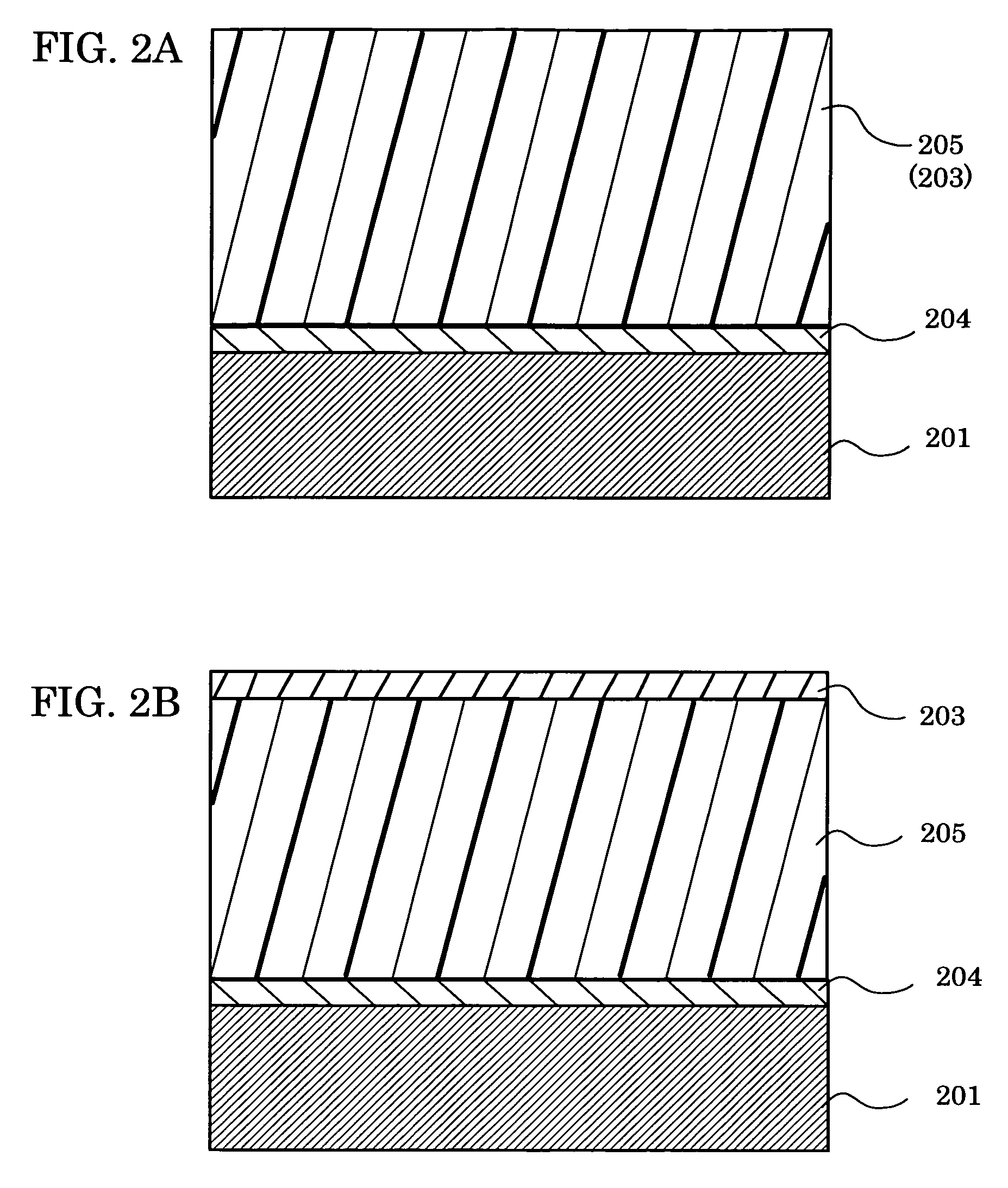
[0204]An undercoat layer was disposed on a support made of aluminum (having an outer diameter of 30 mm) by coating the support with the following coating liquid according to a dip coating so that the undercoat layer had a thickness of 3.5 μm after drying the coating.
[0205]
Composition of Coating LiquidAlkyd resin (manufactured and sold by Dainippon Ink &6partsChemicals Inc.; trade name: Beckozole 1307-60-EL)Melamine resin(manufactured and sold by Dainippon Ink &4partsChemicals Inc.; trade name: Super Beckamine G-821-60)Titanium oxide(manufactured and sold by Ishihara40partsSangyo Kaisha Ltd.; trade name: CR-EL)Methyl ethyl ketone50parts
[0206]A charge generating layer was disposed on the above-disposed undercoat layer by coating the undercoat layer with a coating liquid for disposing the charge generating layer, which comprised a bisazo pigment represented by the following formula according to a dip coating, and the resultant coating was dried by the heating so that the charge generat...
example 2
[0212]The photoconductor of Example 2 was produced in substantially the same manner as in Example 1, except that in the light energy irradiating vessel, air was purged with argon gas until an oxygen concentration was lowered to 0.05 vol % to 0.12 vol %.
example 3
[0213]The photoconductor of Example 3 was produced in substantially the same manner as in Example 1, except that as the radical polymerizable compound having a charge transport structure, Compound No. 182 was used. The thickness of the crosslinked layer of the obtained photoconductor was measured and found to be 4.4 μm.
PUM
 Abstract
Description
Claims
Application Information
 - R&D
- Intellectual Property
- Life Sciences
- Materials
- Tech Scout
- Unparalleled Data Quality
- Higher Quality Content
- 60% Fewer Hallucinations
Browse by: Latest US Patents, China's latest patents, Technical Efficacy Thesaurus, Application Domain, Technology Topic, Popular Technical Reports.
© 2025 PatSnap. All rights reserved.Legal|Privacy policy|Modern Slavery Act Transparency Statement|Sitemap|About US| Contact US: help@patsnap.com


