Organo-electronic functional material and use thereof
a functional material and functional material technology, applied in the field of organoelectronic functional materials, can solve the problems of poor heat resistance of films, poor stability and life, and -mtdata have a heat resistance problem
- Summary
- Abstract
- Description
- Claims
- Application Information
AI Technical Summary
Benefits of technology
Problems solved by technology
Method used
Image
Examples
example 1
Synthesis of 1,3,5-tris(p-tolylamino)benzene
[0048]11.8 g of phloroglucinol, 50 g of p-toluidine and 0.5 g of iodine were placed in a 300 mL capacity three necked flask and the reaction was carried out at a temperature of 150° C. with stirring under a nitrogen atmosphere. After the reaction, the resultant reaction mixture was washed with methanol, hexane and methanol in this order, followed by drying to provide 31.9 g of the desired 1,3,5-tris(p-tolylamino)benzene as slightly reddish solid. The yield was 86.5%.
Synthesis of 1,3,5-tris(N-(4′-methyl-4-biphenylyl)-N-(p-tolyl)amino)-benzene (p-MBTAB)
[0049]2.0 g of 1,3,5-tris(p-tolylamino)benzene, 7.0 g of 4-iodo-4′-methylbiphenyl, 6.9 g of potassium carbonate, 1.0 g of copper powder, 0.7 g of 18-crown-6 (or 1,4,7,10,13,16-hexaoxacyclooctadecane) and 15 mL of mesitylene (reaction solvent) were placed in a 100 mL capacity glass flask and the reaction was carried out at a temperature of 170° C. for 15 hours under a nitrogen atmosphere. After...
example 2
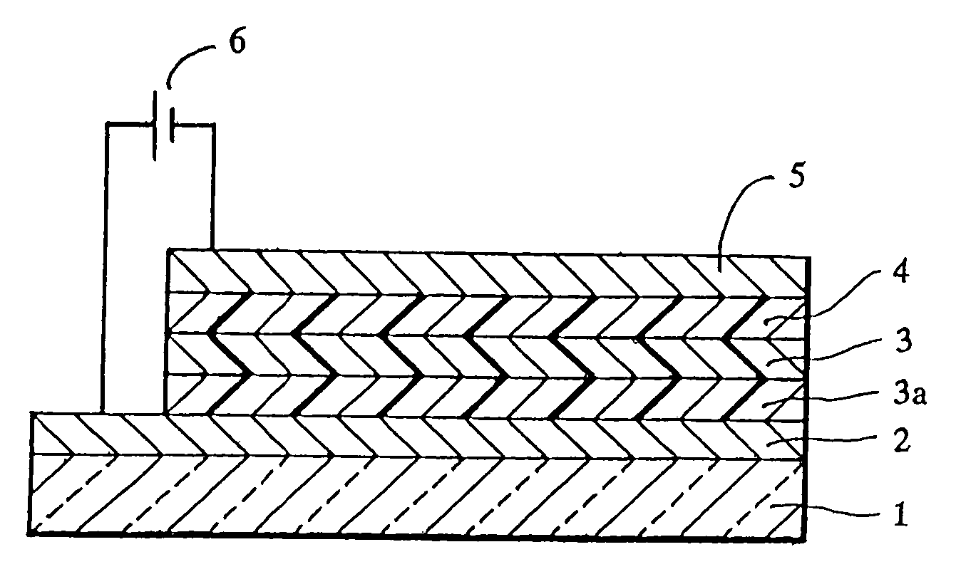
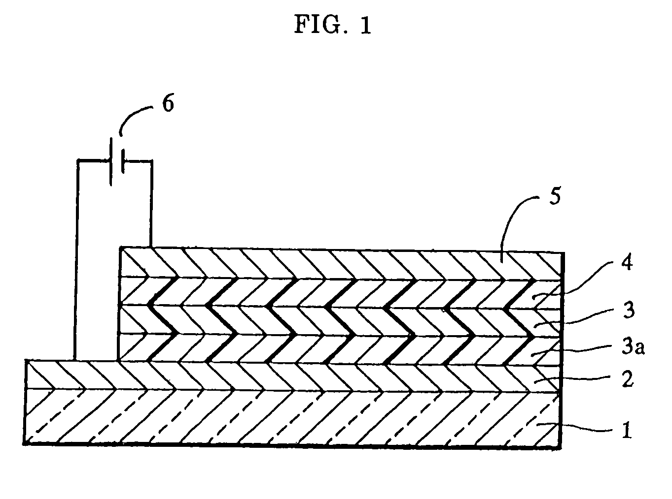
[0062]A sheet of plate glass having an ITO coating on one face (available from Sanyo Vacuum K.K.) was subjected to ultrasonic cleaning using acetone and then steam cleaning using methanol, followed by irradiation with ultraviolet rays by using a low-pressure mercury lamp for 10 minutes. Immediately after the irradiation, copper phthalocyanine (CuPC) was vapor deposited to form a hole injecting layer 20 nm thick and then p-MBTAB was vapor deposited to form a hole transporting layer 40 nm thick in this order on the ITO coating by using a vacuum deposition apparatus. Subsequently, an emission layer 75 nm thick was formed of tris(8-quinolinol)aluminum (Alq3) on the hole transporting layer, and then a lithium fluoride layer 0.5 nm thick and an aluminum layer 100 nm thick were layered in this order on the emission layer to form a cathode, thereby providing an organic electroluminescence element.
[0063]The change of luminance with time was examined by applying voltage across the electrodes ...
example 3
[0066]A sheet of plate glass having an ITO coating on one face (available from Sanyo Vacuum K.K.) was subjected to ultrasonic cleaning using acetone and then steam cleaning using methanol, followed by irradiation with ultraviolet rays by using a low-pressure mercury lamp for 10 minutes. Immediately after the irradiation, 4,4′,4″-tris(N-(2-naphthyl)-N-phenylamino)triphenylamine (2-TNATA) was vapor deposited to form a hole injecting layer 50 nm thick and then p-MBTAB was vapor deposited to form a hole transporting layer 10 nm thick in this order on the ITO coating by using a vacuum deposition apparatus. Subsequently, an emission layer 75 nm thick was formed of tris(8-quinolinol)aluminum (Alq3) on the hole transporting layer, and then a lithium fluoride layer 0.5 nm thick and an aluminum layer 100 nm thick were layered in this order on the emission layer to form a cathode, thereby providing an organic electroluminescence element.
[0067]The voltage-luminance characteristics of the organi...
PUM
| Property | Measurement | Unit |
|---|---|---|
| glass transition temperature | aaaaa | aaaaa |
| glass transition temperature | aaaaa | aaaaa |
| glass transition temperature | aaaaa | aaaaa |
Abstract
Description
Claims
Application Information
 - R&D
- Intellectual Property
- Life Sciences
- Materials
- Tech Scout
- Unparalleled Data Quality
- Higher Quality Content
- 60% Fewer Hallucinations
Browse by: Latest US Patents, China's latest patents, Technical Efficacy Thesaurus, Application Domain, Technology Topic, Popular Technical Reports.
© 2025 PatSnap. All rights reserved.Legal|Privacy policy|Modern Slavery Act Transparency Statement|Sitemap|About US| Contact US: help@patsnap.com


