Nonvolatile memory device
a memory device and non-volatile technology, applied in the direction of semiconductor devices, basic electric elements, electrical appliances, etc., can solve the problems of reducing threshold voltage, data retention characteristic drops, threshold voltage drops, etc., and achieve good data retention characteristic, reduce voltage, and reduce voltage
- Summary
- Abstract
- Description
- Claims
- Application Information
AI Technical Summary
Benefits of technology
Problems solved by technology
Method used
Image
Examples
first embodiment
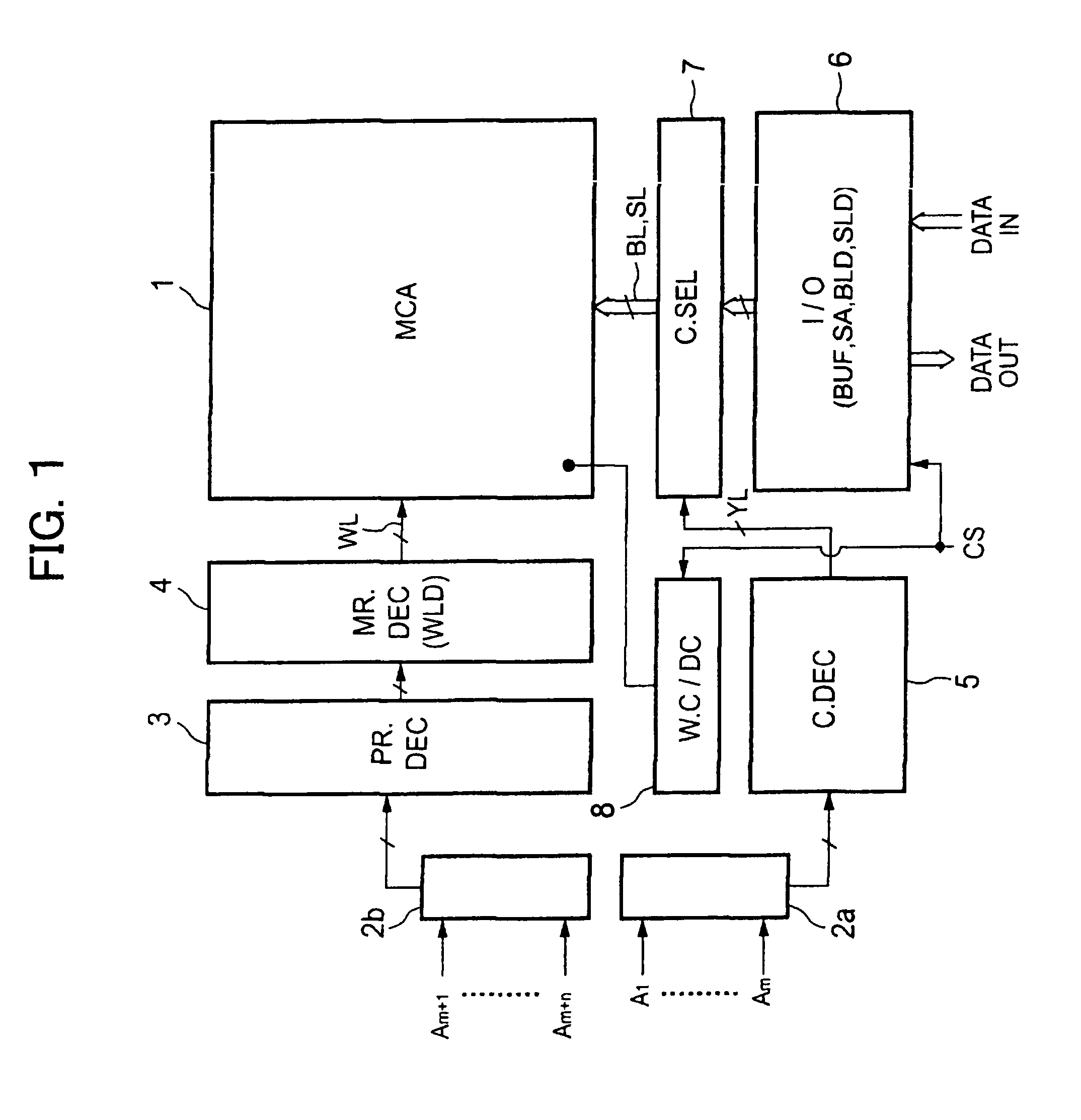
[0067]FIG. 1 is a view of a schematic configuration of a nonvolatile memory device.
[0068]The nonvolatile memory device illustrated in FIG. 1 includes a memory cell array (MCA) 1 having memory transistors arranged in matrix and a memory peripheral circuit for controlling an operation of the memory cell array 1.
[0069]The memory peripheral circuit has a column buffer 2a, a row buffer 2b, a pre-row decoder (PR.DEC) 3, a main-row decoder (MR.DEC) 4, a column decoder (C.DEC) 5, an input and output circuit (I / O) 6, a column selective gate array (C.SEL) 7, and a well charge and discharge circuit (W.C / DC) 8. Note that, in the case of not performing well bias, the well charge and discharge circuit 8 can be omitted. The memory peripheral circuit, not illustrated in the drawing, includes a power source circuit boosting somewhat a power source voltage if necessary and supplying the boosted voltage to the main-row decoder 4 or the well charge and discharge circuit 8, and a control circuit for con...
second embodiment
[0128]In the first embodiment, the evaluation of the charge storage layer (nitride film) is performed by using the Si—H bond density, and the measurement is performed by a spectroscopic ellipsometry method.
[0129]In the present embodiment, a higher accuracy evaluation parameter for the charge storage layer (nitride film) will be proposed and a method of evaluating film quality by using the above parameter and a method of producing a nonvolatile memory device including a step of evaluating the film quality will be described.
[0130]Paid attention to that an refractive index changed depending on a composition rate of the nitride film and a boundary portion between the nitride film and the other film could be identified by using a complex refractive index n*(=n+ik), the inventor investigated that the trap density of the nitride film is monitored by using the complex refractive index n* by a detail experimentation.
[0131]As a result, it was learned that the trap density can be monitored by ...
third embodiment
[0159]In the present embodiment, as a parameter of the nitride film for determining the data retention characteristic, a use of an optical bandgap will be proposed instead of the Si—H bond density, the extinction coefficient k, or absorption coefficients α used in the first and the second embodiment. And, a method of evaluating the film quality and a method of producing a nonvolatile memory device including a step of evaluating the film quality will be described.
[0160]The inventor investigated a relationship between the data retention characteristic and an optical property of the nitride film in detail, as a result, obtained an information that an upper limit of an optical bandgap in the nitride film 12B was demanded to suppress the diffusion of the charge injected locally in the nitride film 12B.
[0161]And, the inventor found that, by the optical bandgap given from the absorption coefficients α of the nitride film, defective or indefectible of the data retention characteristic can b...
PUM
 Abstract
Description
Claims
Application Information
 - R&D
- Intellectual Property
- Life Sciences
- Materials
- Tech Scout
- Unparalleled Data Quality
- Higher Quality Content
- 60% Fewer Hallucinations
Browse by: Latest US Patents, China's latest patents, Technical Efficacy Thesaurus, Application Domain, Technology Topic, Popular Technical Reports.
© 2025 PatSnap. All rights reserved.Legal|Privacy policy|Modern Slavery Act Transparency Statement|Sitemap|About US| Contact US: help@patsnap.com


