
Ge precursor, GST thin layer formed using the same, phase-change memory device including the GST thin layer, and method of manufacturing the GST thin layer

a technology of gst and precursor, which is applied in the direction of germanium organic compounds, organic chemistry, coatings, etc., to achieve good performance characteristics

Active Publication Date: 2009-04-14
SAMSUNG ELECTRONICS CO LTD
View PDF12 Cites 23 Cited by
  • Summary
  • Abstract
  • Description
  • Claims
  • Application Information

AI Technical Summary

Benefits of technology

The present invention provides a method for manufacturing a thin layer of a material called GST, which is used in phase-change memory devices. The method involves depositing a precursor containing Ge, N, and Si at a low temperature, followed by a process of heat treatment to form the GST thin layer. The resulting thin layer has a uniform thickness and low reset current, making it suitable for various devices. The technical effect of this invention is to improve the performance of phase-change memory devices by providing a high-quality GST thin layer with good performance characteristics.

Problems solved by technology

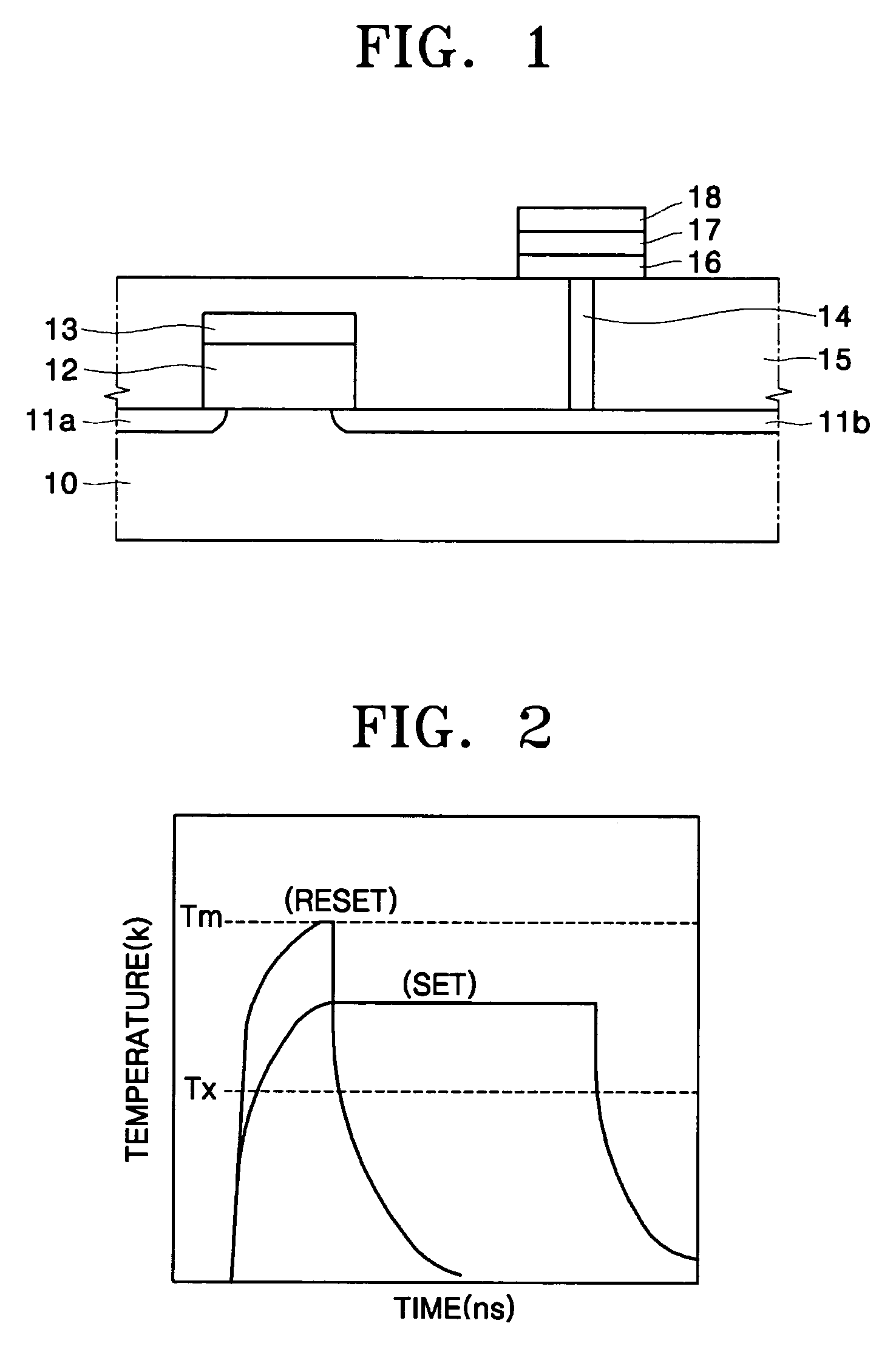
In order to increase the temperature to Tm, a large amount of a current must be supplied, which is undesirable for a highly integrated memory device.

Method used


Image

  • Ge precursor, GST thin layer formed using the same, phase-change memory device including the GST thin layer, and method of manufacturing the GST thin layer
  • Ge precursor, GST thin layer formed using the same, phase-change memory device including the GST thin layer, and method of manufacturing the GST thin layer
  • Ge precursor, GST thin layer formed using the same, phase-change memory device including the GST thin layer, and method of manufacturing the GST thin layer

Examples


embodiments

Embodiment 1

[0062]

[0063]In Reaction Scheme 1, a solution of 0.1 moles of hexamethyldisilazane in 1000 ml of hexane and 0.2 mole of nBu—Li were mixed at room pressure and −78°, and then reacted for 4 hours at room temperature. As a result, the compound of formula 3′ was produced.

[0064]

[0065]In Reaction Scheme 2, 0.5 mole of the compound of formula 3′ and 0.1 mole of GeCl4 were mixed in 1000 ml of THF, reacted at 150° C. for 8 hours, and dried in a vacuum at room temperature. The resultant product was purified by fractional distillation at 0.1 torr and 60° C. to obtain 38 g of the compound of formula 3, that is, Ge[N(Si(CH3)3)2]4. Then, the compound of formula 3 was identified by 1H-NMR and 13C-NMR, all of which were performed at 25° C. with C6D6. The results are shown in FIGS. 5A and 5B, respectively. Referring to FIGS. 5a and 5b, the presence of a Ge—N bond and a N—Si bond in the compound of formula 3 can be confirmed. The compound of formula 3 refers to a Ge precursor 1.

example 1

MEASUREMENT EXAMPLE 1

Thermal Decomposition Characteristics

[0068]The thermal decomposition characteristics of Ge precursors A, B, and 1 were measured. The results are shown in FIG. 6. The thermal decomposition was performed at 400° C. in a He atmosphere in an injection chamber system. The results were measured using gas chromatography. In FIG. 6, (a) illustrates a peak of Ge(CH3)4 that is the Ge precursor A, (b) illustrates a peak of Ge[N(CH3)2]4 that is the Ge precursor B, and (c) illustrates a peak of Ge[N(Si(CH3)3)2]4 that is the Ge precursor 1. Comparing (c) to (a) and (b), it was confirmed that the Ge precursor 1 according to an embodiment of the present invention decomposed in a shorter time than Ge precursors A and B. That is, since the rate of thermal decomposition of Ge precursor 1 according to an embodiment of the preset invention is higher than those of the conventional Ge precursors A and B, the Ge precursor 1 is more suitable for CVD or ALD.

example 2

MEASUREMENT EXAMPLE 2

Layer Forming Ability at a Low Temperature

[0069]The layer forming ability was measured using the Ge precursor A, and the Ge precursor 1. At this time, ALD was used. First, under deposition conditions shown in Table 1 below, a Ge thin layer was formed by ALD using Ge precursor A. Separately, a Ge thin layer doped with N and Si was formed using the Ge precursor 1 under the conditions and the method described above. Then, SEM images of cross sections of the two Ge thin layers were taken. The results are shown in FIGS. 7A and 7B. In particular, H2 was used as shown in Table 1.

[0070]

TABLE 1Deposition Temperature250° C.Deposition Cycle250 timesProcessing Period0.006 / 3 / 1 / 1Ar influx500 sccmH2 influx300 sccm

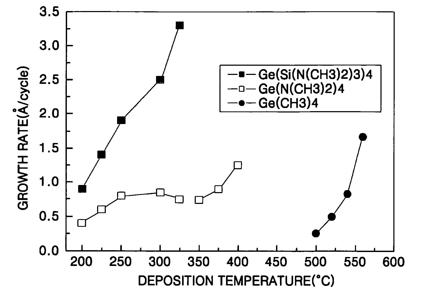
[0071]Referring to FIG. 7A, forming a Ge thin layer was not properly achieved because the deposition temperature is low, such as 250° C. shown in Table 1. Referring to FIG. 7B, the Ge thin layer formed from the Ge precursor 1 was formed to a thickness of about 330 Å a...


PUM

PropertyMeasurementUnit
temperatureaaaaaaaaaa
reset currentaaaaaaaaaa

Abstract

Provided are a Ge precursor for low temperature deposition containing Ge, N, and Si, a GST thin layer doped with N and Si formed using the same, a memory device including the GST thin layer doped with N and Si, and a method of manufacturing the GST thin layer. The Ge precursor for low temperature deposition contains N and Si such that the temperature at which the Ge precursor is deposited to form a thin layer, particularly, the GST thin layer doped with N and Si, can be low. In addition, during the low temperature deposition, H2 plasma can be used. The GST phase-change layer doped with N and Si formed from the Ge precursor for low temperature deposition has a low reset current. Therefore, a memory device including the GST phase-change layer doped with N and Si can be highly integrated, have a high capacity, and can be operated at a high speed.

Description

BACKGROUND OF THE DISCLOSURE[0001]This application claims the benefit of Korean Patent Application No. 10-2004-0112906, filed on Dec. 27, 2004, in the Korean Intellectual Property Office, the disclosure of which is incorporated herein in its entirety by reference.[0002]1. Field of the Disclosure[0003]The present disclosure relates to a Ge precursor, a GST thin layer formed using the same, and a method of manufacturing the GST thin layer, and more particularly, to a Ge precursor for low temperature deposition containing Ge, N, and Si, a GST thin layer formed at a low temperature using the Ge precursor, a phase-change memory device including the GST thin layer, and a method of manufacturing the GST thin layer.[0004]2. Description of the Related Art[0005]Phase-change materials exist in a crystalline state or an amorphous state according to temperature. A phase-change material has a lower resistance and a more ordered atomic arrangement in a crystalline state than in an amorphous state....

Claims


Application Information

Patent Timeline
Patent Type & Authority Patents(United States)
IPC IPC(8): C07F7/08C07F7/00C23C16/00
CPCC07F7/10C07F7/30C23C16/305H01L27/2436H01L45/06H01L45/1233H01L45/144H01L45/1616H10B63/30H10N70/231H10N70/826H10N70/8828H10N70/023
Inventor SEO, BUM-SEOKLEE, JUNG-HYUN
Owner SAMSUNG ELECTRONICS CO LTD
Learn More